October 1, 2024

Analog Electronics Chapter 1: Operational Amplifiers Explained — Basics to Applications

An amplifier is an electronic device or circuit that increases the power, voltage, or current of an input signal. Amplifiers are a crucial part of many electronic systems, enabling small input signals to be boosted for a variety of applications such as audio devices, communication systems, and instrumentation.

At its core, an amplifier takes a weak input signal and, through its design, produces a stronger output signal while maintaining the characteristics of the input, such as waveform and frequency. This increase in signal strength can be described by the term “gain,” which represents how much an amplifier increases the amplitude of the signal.

The gain of a single amplifier is often insufficient for practical use. To achieve the desired high gain, multiple amplifier stages are coupled together.

An operational amplifier (OPAMP) is a high-gaindirect current (DC) amplifier with differential inputs. It amplifies the difference between two identical but opposite input signals while rejecting common-mode signals (signals that are the same at both inputs). This makes OPAMPs very versatile, as they can amplify both DC and alternating current (AC) signals.

Additionally, OPAMPs can perform various mathematical operations, such as addition, subtraction, differentiation, integration, and even act as buffers or analog-to-digital (A/D) converters. OPAMPs typically require a dual power supply for proper functioning.

Characteristics of an ideal OPAMP:

  1. Infinite open-loop gain
  2. Infinite input impedance
  3. Zero output impedance
  4. Infinite common-mode rejection ratio (CMRR)
  5. Zero response time (instantaneous response)
  6. Zero input bias current
  7. Zero input offset current
  8. Zero input offset voltage

Basic Circuit Diagram of an OPAMP
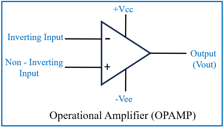
The diagram above shows the basic circuit of an operational amplifier (OPAMP). It has two input terminals — an inverting input (labeled “-”) and a non-inverting input (labeled “+”) — and one output terminal. The inputs are differential, meaning the OPAMP amplifies the voltage difference between the two input terminals. The inverting input reverses the phase of the input signal by 180 degrees, while the non-inverting input maintains the signal’s original phase.

  1. Inverting Input (-): The signal applied to this input will be inverted at the output.
  2. Non-inverting Input (+): The signal applied to this input will appear at the output without inversion.

In addition to the inputs and the output, the OPAMP requires a power supply to operate. This is provided by the +Vcc and -Vee terminals:

  1. +Vcc: The positive supply terminal, which provides the upper voltage limit for the output signal. The output cannot exceed this voltage.
  2. -Vee: The negative supply terminal, which sets the lower voltage limit for the output signal. The output cannot drop below this voltage.

For example, if the OPAMP is powered by +15V and -15V, the output can swing between these limits. This is essential for amplifying both positive and negative signals, making the OPAMP suitable for alternating current (AC) signals as well as direct current (DC) signals.

Block Diagram of an Operational Amplifier (OPAMP)

The operational amplifier (OPAMP) consists of several internal blocks that work together to amplify the input signal. Below is the step-by-step flow and function of each block in your block diagram:

1. Differential Amplifier (First Stage):

The two input signals, inverting and non-inverting, are fed into the first differential amplifier. This stage amplifies the difference between the two inputs and rejects any signals common to both inputs (common-mode signals).
The constant current source connected to this stage provides stable biasing for the transistors in the differential pair. It ensures that the current remains constant regardless of variations in supply voltage or temperature, improving the amplifier’s linearity and performance.
This stage sets the foundation for the OPAMP’s high input impedance and good common-mode rejection ratio (CMRR).

2. Second Differential Amplifier (Intermediate Stage):

The output from the first differential amplifier is fed into a second differential amplifier, which further amplifies the differential signal while continuing to reject any residual common-mode noise.
This stage improves the gain of the OPAMP and ensures that the signal is prepared for the next stages of amplification and processing.

3. Emitter Follower (Buffer Stage):

After the second differential amplifier, the signal is passed to an emitter follower (or buffer) stage. This stage has a high input impedance and low output impedance, making it ideal for impedance matching.
The emitter follower ensures that the signal can be transferred efficiently to the next stages without loading the previous stage, maintaining signal integrity.

4. DC Level Shifter:

The DC level shifter is used to adjust the DC bias of the signal. Since the differential amplifier stages might introduce a DC offset, the level shifter corrects this by shifting the signal back to the desired reference level.
This block ensures that the output stage operates correctly, especially in circuits where precise voltage levels are critical.

5. Output Stage:

The output stage is typically a high-power amplifier stage that provides the necessary current to drive the load connected to the OPAMP’s output.
This stage is designed to handle large signal swings and provide enough current to low-impedance loads, ensuring that the OPAMP can drive a variety of external circuits.

6. Output Load:

The final block is the output load, which represents the external circuit or device that the OPAMP is driving. This could be anything from another amplifier stage to a speaker or other analog component.
Each stage in the OPAMP works together to provide high gain, low output impedance, and excellent signal fidelity, ensuring the amplified signal is clean and stable across a wide range of applications.

Conclusion and What’s Next

In this blog, we’ve explored the fundamental aspects of operational amplifiers (OPAMPs), from their basic functionality and characteristics to the internal block diagram and circuit structure. Understanding these components is crucial for grasping the power and versatility of OPAMPs in electronic systems.

In the next blog, we’ll dive deeper into specific OPAMP configurations such as inverting and non-inverting amplifiers, where we’ll explain how these modes work. Additionally, we’ll explore important OPAMP parameters such as:

  1. Common-Mode Rejection Ratio (CMRR): The ability of an OPAMP to reject input signals common to both input terminals.
  2. Power Supply Rejection Ratio (PSRR): The OPAMP’s ability to maintain performance despite variations in the power supply.
  3. Slew Rate: The rate at which an OPAMP’s output can change in response to a rapid input signal.

We’ll also look at how OPAMPs perform different operations, such as:

  1. Addition and Subtraction
  2. Differentiation and Integration
  3. Buffering
  4. Analog-to-Digital Conversion (A/D)

Stay tuned to understand how these operations and configurations make OPAMPs an indispensable tool in modern electronics!
September 16, 2024

Decoding the Decoder: A Deep Dive into Digital Logic

In the world of digital systems, data transmission and processing depend on the conversion and manipulation of binary data. Just as encoders convert information from one format into another, decoders serve the reverse function: they translate encoded data back into its original form. Decoders are essential in numerous applications, from simple digital circuits to complex communication systems. In this blog, we will explore what decoders are, how they work, and where they are used.

What is a Decoder?

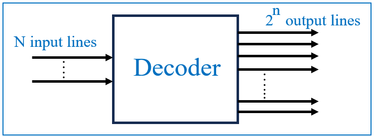
A decoder is a combinational logic circuit that converts coded inputs into coded outputs. More specifically, a decoder takes a binary input (often in the form of n inputs) and produces an output based on the input combination. The output is typically an active signal on one of its multiple output lines, corresponding to the binary input pattern.

In simple terms, while an encoder compresses data into a smaller number of bits, a decoder expands those bits back to their original form, recovering the original information.

A basic decoder performs the reverse operation of an encoder. It takes an n-bit binary input and provides up to 2^n unique output lines. This feature makes decoders highly useful in applications where a specific output needs to be activated based on a binary input code.

For example, a 2-to-4 decoder has two input lines (A0, A1) and four output lines (Y0, Y1, Y2, Y3). It converts the 2-bit binary input into a unique active output line. Each combination of the input corresponds to one of the output lines being activated, while the others remain inactive.

Types of Decoders

Decoders come in various configurations based on the number of inputs and outputs. The most common types include:

  • 2-to-4 Decoder: As described above, a 2-bit input produces four possible outputs.
  • 3-to-8 Decoder: A 3-bit input results in eight possible outputs, often used in memory address decoding.
  • 4-to-16 Decoder: Expanding further, a 4-bit input activates one of sixteen outputs, commonly used in microprocessors for selecting memory locations or devices.

In some applications, decoders may also include enable inputs that allow or block the decoding function.

Working Principle of a Decoder

The function of a decoder can be understood through its basic logic structure. Consider a 2-to-4 decoder, one of the simplest forms of decoders. It takes a 2-bit binary input and activates one of four output lines based on the input combination:

  • Input: 00 → Output Line 0 is active
  • Input: 01 → Output Line 1 is active
  • Input: 10 → Output Line 2 is active
  • Input: 11 → Output Line 3 is active

Each output is mapped to a specific input combination, typically using AND gates. The truth table of the 2-to-4 decoder demonstrates this operation:

Thus, depending on the binary value of the input, only one output line is active at any given time.

Block Diagram and Logic Circuit Explanation

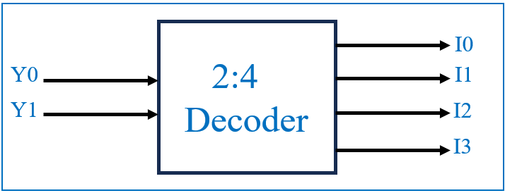
The block diagram below shows a basic 2:4 decoder with two inputs (Y0Y1) and four outputs (I0I1I2I3):

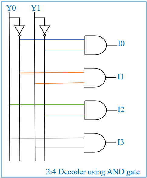
This decoder activates a specific output based on the combination of the input values. The internal circuit uses AND gates and NOT gates to realize the function. Each output is connected to a specific combination of inputs, as shown in the logic diagram below:

In this logic circuit:

  • I0 is activated when both Y1 and Y0 are low (00), utilizing a NOT gate on both inputs before sending them to the AND gate.
  • I1 is activated when Y1 is low and Y0 is high (01).
  • I2 is activated when Y1 is high and Y0 is low (10).
  • I3 is activated when both Y1 and Y0 are high (11).

The following equations describe each output:

  • I0 = ~Y1 & ~Y0 (Active when both inputs are 00)
  • I1 = ~Y1 & Y0 (Active when the input is 01)
  • I2 = Y1 & ~Y0 (Active when the input is 10)
  • I3 = Y1 & Y0 (Active when both inputs are 11)

Verilog Code for 2-to-4 Decoder

Here’s a simple Verilog code for a 2-to-4 binary decoder:

module decoder_2to4 (
input wire A0, // First input bit
input wire A1, // Second input bit
output wire Y0, // Output line 0
output wire Y1, // Output line 1
output wire Y2, // Output line 2
output wire Y3 // Output line 3
);

// Logic for the decoder using continuous assignment
assign Y0 = ~A1 & ~A0; // Active when A1A0 is 00
assign Y1 = ~A1 & A0; // Active when A1A0 is 01
assign Y2 = A1 & ~A0; // Active when A1A0 is 10
assign Y3 = A1 & A0; // Active when A1A0 is 11
endmodule

Applications of Decoders

Decoders are used extensively in digital electronics and communication systems. Some common applications include:

  • Memory Address Decoding: Decoders are used in microprocessors and memory systems to select specific memory locations. A decoder decodes the binary address provided by the CPU, activating the corresponding memory location for reading or writing data.
  • Seven-Segment Display: A special type of decoder converts binary or BCD (Binary-Coded Decimal) data into signals that light up specific segments of a seven-segment display, representing numbers.
  • Data Demultiplexing: Decoders can act as demultiplexers, routing a single input signal to one of many output lines based on the input address.
  • Instruction Decoding: In CPUs, decoders are used to interpret machine code instructions and activate the appropriate circuitry to execute each command.
  • Communication Systems: Decoders play a vital role in converting encoded signals back into their original form, enabling correct data reception.

Conclusion

Decoders are indispensable in digital electronics, facilitating the process of translating coded information back into a usable form. From enabling memory selection in computers to powering seven-segment displays, decoders are everywhere in modern technology. By understanding the principles behind decoders, you gain deeper insights into how data is processed and transmitted in digital systems.

Whether you’re building a simple logic circuit or designing complex communication protocols, understanding decoders is essential to mastering digital electronics.

September 6, 2024

Understanding the Full Subtractor: The Complete Subtraction Solution in Digital Electronics

In digital electronics, subtraction is as essential as addition, particularly when dealing with multi-bit numbers. While the Half Subtractor covers basic single-bit subtraction, it falls short when borrow operations come into play. The Full Subtractor is designed to handle these situations, making it a crucial element in advanced digital systems. This blog post will explore the Full Subtractor, its components, operation, and significance.

What is a Full Subtractor?

A Full Subtractor is a combinational circuit that performs the subtraction of two binary bits while accounting for a borrow from a previous stage. Unlike the Half Subtractor, which handles subtraction without borrow consideration, the Full Subtractor manages both the difference and borrow efficiently in multi-bit binary subtraction. It produces two outputs:

  • Difference (D)
  • Borrow (B_out)

Theoretical Background

Let’s revisit the rules of binary subtraction, adding the case where we borrow from a previous operation:

  • 0–0 = 0
  • 1–0 = 1
  • 1–1 = 0
  • 0–1 = 1 (with a borrow of 1)

When performing multi-bit subtraction, the Full Subtractor must also consider an input borrow (B_in) from the previous less significant bit, leading to more complex calculations.

Components of a Full Subtractor

A Full Subtractor involves three binary inputs:

  • A: The minuend (the number being subtracted from)
  • B: The subtrahend (the number being subtracted)
  • B_in: The borrow input from the previous stage

The Full Subtractor employs the following logic gates:

  • XOR Gates: To compute the difference
  • AND and OR Gates: To compute the borrow output

The logic expressions for the outputs are:

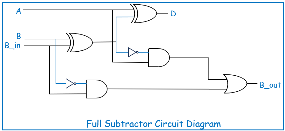
  • Difference (D) = A ⊕ B ⊕ B_in
  • Borrow out (B_out) = (A’ ANDB) OR ((A ⊕ B)’ AND B_in)

Circuit Diagram

The Full Subtractor circuit is built using the above components, showing how the XOR gates compute the difference and how the AND/OR gates handle the borrow. Here’s a simplified diagram for better understanding:

Truth Table

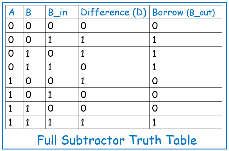
The Full Subtractor truth table details the results of all possible combinations of the three inputs (A, B, and B_in):

Applications of Full Subtractor

The Full Subtractor is vital in systems requiring multi-bit subtraction, including:

  • Arithmetic Logic Units (ALUs): A core component in CPUs for handling multi-bit arithmetic operations.
  • Digital Counters: Used in applications that require down-counting, where the Full Subtractor helps manage borrow operations.
  • Binary Calculators: Necessary for performing precise binary arithmetic.
  • Data Processing Systems: In systems requiring complex binary operations, the Full Subtractor plays a key role in ensuring accurate computations.

Conclusion

The Full Subtractor extends the functionality of the Half Subtractor by accounting for borrow operations, making it indispensable in multi-bit subtraction scenarios. Understanding the Full Subtractor’s logic and applications is essential for advancing in digital circuit design and gaining a deeper insight into how subtraction is handled in various digital systems. As you move toward more complex circuits, mastering the Full Subtractor will provide a strong foundation for future exploration in digital electronics.

Explore Our Topics!

Check out the extensive list of topics we discuss:  Communication Protocols: -  USB   - RS232   -  Ethernet   -  AMBA Protocol: APB, AHB and...