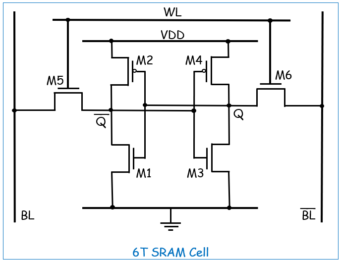
A static random-access memory (SRAM) cell typically uses several transistors to store a single bit of data. The exact number of transistors depends on the specific design and technology node used in the SRAM cell. However, a common configuration for an SRAM cell in modern integrated circuits (ICs) includes six transistors.
These six transistors are arranged in a cross-coupled flip-flop configuration, which forms the basic storage element of the SRAM cell. A typical SRAM cell, as shown in above figure, consists of six transistors (often referred to as a 6T-SRAM cell). These transistors are organized into access transistors (M5 and M6), pull-up transistors (M2 and M4), and pull-down transistors (M1 and M3). SRAM operations include hold, read, and write operations:
- Hold Operation: During hold operation, both access transistors are turned OFF, and SRAM maintains its current state due to latching.
- Read Operation: During read operation, the two bit lines must be recharged to VDD, and the access transistors are turned on. The sense amplifier detects the potential difference between the bit lines, determining the stored data as logic one or logic zero.
- Write Operation: In the write operation, data is written onto the memory by applying it to the bit line while the access transistors are in the on state.
