Showing posts with label digital electronics. Show all posts

September 6, 2024

Understanding the Full Subtractor: The Complete Subtraction Solution in Digital Electronics

In digital electronics, subtraction is as essential as addition, particularly when dealing with multi-bit numbers. While the Half Subtractor covers basic single-bit subtraction, it falls short when borrow operations come into play. The Full Subtractor is designed to handle these situations, making it a crucial element in advanced digital systems. This blog post will explore the Full Subtractor, its components, operation, and significance.

What is a Full Subtractor?

A Full Subtractor is a combinational circuit that performs the subtraction of two binary bits while accounting for a borrow from a previous stage. Unlike the Half Subtractor, which handles subtraction without borrow consideration, the Full Subtractor manages both the difference and borrow efficiently in multi-bit binary subtraction. It produces two outputs:

  • Difference (D)
  • Borrow (B_out)

Theoretical Background

Let’s revisit the rules of binary subtraction, adding the case where we borrow from a previous operation:

  • 0–0 = 0
  • 1–0 = 1
  • 1–1 = 0
  • 0–1 = 1 (with a borrow of 1)

When performing multi-bit subtraction, the Full Subtractor must also consider an input borrow (B_in) from the previous less significant bit, leading to more complex calculations.

Components of a Full Subtractor

A Full Subtractor involves three binary inputs:

  • A: The minuend (the number being subtracted from)
  • B: The subtrahend (the number being subtracted)
  • B_in: The borrow input from the previous stage

The Full Subtractor employs the following logic gates:

  • XOR Gates: To compute the difference
  • AND and OR Gates: To compute the borrow output

The logic expressions for the outputs are:

  • Difference (D) = A ⊕ B ⊕ B_in
  • Borrow out (B_out) = (A’ ANDB) OR ((A ⊕ B)’ AND B_in)

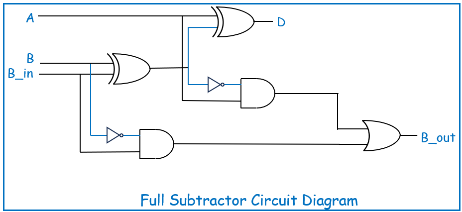
Circuit Diagram

The Full Subtractor circuit is built using the above components, showing how the XOR gates compute the difference and how the AND/OR gates handle the borrow. Here’s a simplified diagram for better understanding:

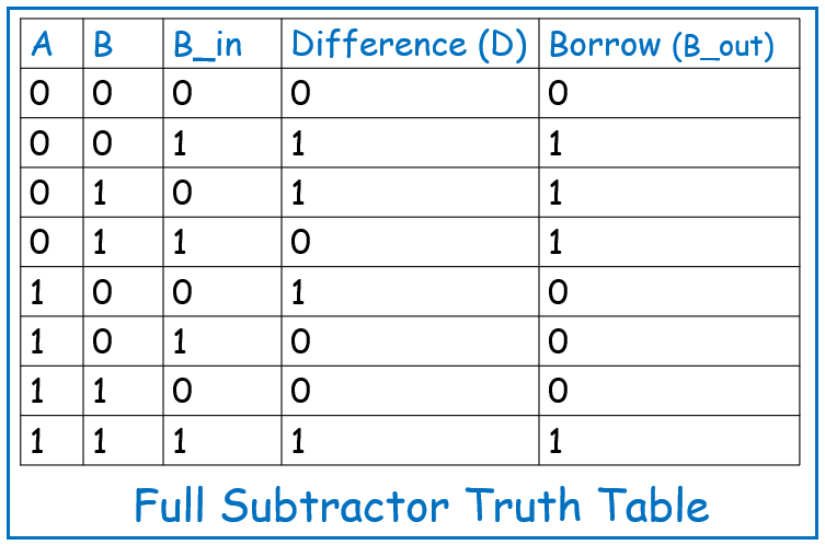
Truth Table

The Full Subtractor truth table details the results of all possible combinations of the three inputs (A, B, and B_in):

Applications of Full Subtractor

The Full Subtractor is vital in systems requiring multi-bit subtraction, including:

  • Arithmetic Logic Units (ALUs): A core component in CPUs for handling multi-bit arithmetic operations.
  • Digital Counters: Used in applications that require down-counting, where the Full Subtractor helps manage borrow operations.
  • Binary Calculators: Necessary for performing precise binary arithmetic.
  • Data Processing Systems: In systems requiring complex binary operations, the Full Subtractor plays a key role in ensuring accurate computations.

Conclusion

The Full Subtractor extends the functionality of the Half Subtractor by accounting for borrow operations, making it indispensable in multi-bit subtraction scenarios. Understanding the Full Subtractor’s logic and applications is essential for advancing in digital circuit design and gaining a deeper insight into how subtraction is handled in various digital systems. As you move toward more complex circuits, mastering the Full Subtractor will provide a strong foundation for future exploration in digital electronics.

July 1, 2024

Understanding the Half Subtractor: Essential Basics in Digital Electronics

In the realm of digital electronics, efficient subtraction operations are just as crucial as addition. The Half Subtractor, akin to its counterpart, the Half Adder, serves as a fundamental component in processing binary numbers. This blog post aims to elucidate the Half Subtractor, its operational principles, components, and significance in digital circuit design.

What is a Half Subtractor?

A Half Subtractor is a digital circuit designed to perform the subtraction of two single-bit binary numbers. Unlike the Full Subtractor, which handles borrow operations for multi-bit subtraction, the Half Subtractor operates without considering borrow. It produces two outputs: a difference bit (D) and a borrow bit (B).

Theoretical Background

Before delving into the Half Subtractor’s intricacies, let’s recap binary subtraction basics:

  • 0–0 = 0
  • 1–0 = 1
  • 1–1 = 0
  • 0–1 = 1 (with a borrow of 1)

Components of a Half Subtractor

A Half Subtractor comprises two essential logic gates:

  • XOR Gate: Computes the difference bit (D).
  • AND Gate: Computes the borrow bit (B).

The logical expressions governing these outputs are:

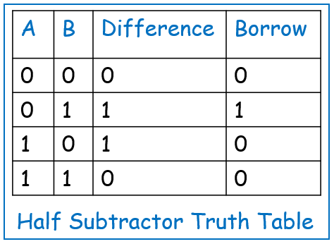
  • Difference (D) = A XOR B
  • Borrow (B) = A’ AND B

Here, A and B represent the binary inputs, and A’ denotes the complement of A.

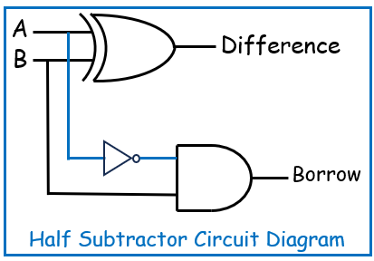
Circuit Diagram

The circuit diagram for a Half Subtractor is straightforward, employing an XOR gate and an AND gate arranged as follows:

Truth Table

The truth table below illustrates the functionality of the Half Subtractor for all possible input combinations:

Applications of Half Subtractor

Half Subtractors find various applications in digital systems, including:

  • Building Full Subtractors: Essential for multi-bit subtraction operations, using Full Subtractors constructed from Half Subtractors.
  • ALUs (Arithmetic Logic Units): Integral to microprocessor design, where subtraction operations are crucial for arithmetic and logical calculations.
  • Binary calculators and digital counters: Used in devices requiring precise counting and data manipulation capabilities.
  • Error Detection: Utilized in checksum calculations for ensuring data integrity in communication and storage systems.

Conclusion

In summary, the Half Subtractor plays a pivotal role in digital electronics, facilitating the fundamental operation of binary subtraction. Its simplicity and essential function make it an indispensable component in the construction of more complex digital circuits. By grasping the operational principles and applications of the Half Subtractor, one gains a solid foundation in digital logic design, essential for advancing to more intricate digital systems and applications.

June 19, 2024

Why mux is called universal logic selector?

Multiplexers (MUXs) are often called “universal logic selectors” because they can perform a wide range of logical operations and are highly adaptable in digital circuit design. Here’s what makes this title appropriate:

  1. Data Selection Capability: A MUX can select one of several input signals and route it to a single output line based on control signals (selection lines). This makes it highly versatile for various data routing and signal selection tasks within digital systems.
  2. Flexibility in Applications: MUXs are used in various applications such as data routing, signal switching, arithmetic operations, and more. Their ability to dynamically select inputs based on control signals makes them a flexible component in digital electronics.
  3. Implementation of Logic Functions: A MUX can be configured to implement any logical function by setting the input lines and selection lines correctly. For instance, a 2^n-to-1 MUX can perform any n-variable Boolean function, which makes it invaluable in designing complex logic circuits.
  4. Reduction of Circuit Complexity: Multiplexers can simplify the design of digital circuits by reducing the number of logic gates needed to implement certain functions. This helps in optimizing the circuit in terms of space and power consumption.
  5. Simplification of Design Process: The use of MUXs can streamline the design process for complex logic circuits. Designers can use MUXs to modularize and simplify the implementation of various logic functions, making the design process more efficient.
  6. Support for Multiple Functions: A single MUX can perform multiple functions depending on how the inputs are configured. This multifunctionality is one of the key reasons MUXs are considered universal logic selectors.

Overall, the multiplexer’s ability to efficiently select, route, and implement a wide range of logical functions in digital circuits is why it is often referred to as a universal logic selector.

June 16, 2024

Understanding the Half Adder: A Fundamental Building Block in Digital Electronics.

In the realm of digital electronics, the ability to perform arithmetic operations is crucial. Among the fundamental components that enable these operations are adders, with the Half Adder being one of the simplest yet essential types. This blog will explore the Half Adder, its components, functionality, and significance in digital circuit design.

What is a Half Adder?

A Half Adder is a digital circuit that performs the addition of two single-bit binary numbers. It produces two outputs: a sum bit and a carry bit. The simplicity of the Half Adder makes it a fundamental building block for more complex arithmetic circuits, such as Full Adders and arithmetic logic units (ALUs).

Theoretical Background

Before delving into the Half Adder, it is essential to understand the basics of binary addition. In binary arithmetic:

  1. 0 + 0 = 0
  2. 0 + 1 = 1
  3. 1 + 0 = 1
  4. 1 + 1 = 10 (which is 0 with a carry of 1)

Components of a Half Adder

A Half Adder consists of two primary components:

  • XOR Gate: Produces the sum bit.
  • AND Gate: Produces the carry bit.

The logical expressions for the outputs are:

  • Sum (S) = A XOR B
  • Carry © = A AND B

Circuit Diagram

The circuit diagram of a Half Adder is straightforward, with an XOR gate and an AND gate connected as shown below:

Truth Table

The truth table below illustrates how the Half Adder operates for all possible input combinations:

Applications of Half Adder

Half Adders are fundamental components in digital electronics and have several applications, primarily in the construction of more complex arithmetic circuits. Here are some key applications:

  1. Building Full Adders: Half Adders are used to construct Full Adders, which can add binary numbers of more than one bit. A Full Adder adds three bits (two significant bits and a carry bit) and produces a sum and a carry bit. By cascading multiple Full Adders (which themselves are built from Half Adders), you can create circuits capable of adding multi-bit binary numbers. This forms the basis of ripple-carry adders and other multi-bit adder architectures.
  2. Arithmetic Logic Units (ALUs): Half Adders are integral to the design of ALUs, which perform a variety of arithmetic and logical operations in microprocessors and digital systems. ALUs use Half Adders and Full Adders to perform binary addition, which is a fundamental operation in computing.
  3. Digital Signal Processing (DSP): Efficient Data Manipulation: In DSP applications, Half Adders are used for efficient data manipulation and processing tasks that require binary addition. Simple binary calculators use Half Adders to perform basic addition operations. They serve as the foundational units that enable binary addition in these devices.
  4. Memory Address Calculation: In memory systems, Half Adders help in the calculation of memory addresses during read and write operations, ensuring data is stored and retrieved correctly.
  5. Digital Counters: Half Adders are used in digital counters, where they help in performing the increment operations necessary for counting sequences.
  6. Encoders and Decoders: In encoders and decoders, Half Adders assist in converting data between different binary codes, which is essential in various digital communication and storage systems.
  7. Error Detection and Correction: Half Adders are used in generating checksums for error detection and correction in data transmission. They help in adding binary values to produce checksums that verify data integrity.

Conclusion

The Half Adder is a fundamental component in digital electronics, serving as a building block for more complex arithmetic circuits. Its simplicity and essential role in binary addition make it a critical topic for anyone studying digital logic design. Understanding the functionality, applications, and implementation of the Half Adder provides a solid foundation for exploring more advanced digital circuits.

For those interested in practical implementations, I have detailed blogs on how to implement a Half Adder using both VHDL and Verilog on Xilinx Vivado. Click on the links below to explore the full implementations and testbench code:

Stay tuned for more detailed blogs on combinational circuits and other key topics in digital electronics.

Why mux is called data selector?

A Multiplexer (MUX) is often called a “data selector” because it chooses one of several input data lines and routes the selected data to a single output line. This function is essential in digital systems for managing and directing data flow. Here are the detailed reasons why a MUX is referred to as a data selector:

  1. Selection of Input Data: A MUX has multiple input lines but only one output line. The selection lines (control signals) determine which input line’s data will be sent to the output. This ability to select and route specific data from many inputs is why it is called a data selector.
  2. Controlled Routing: The selection lines control which input is connected to the output. By changing the values on the selection lines, different inputs can be routed to the output, effectively selecting which data to pass through.
  3. Versatility in Data Management: Multiplexers are used in various applications where it is necessary to choose between different data sources. This includes data routing, signal multiplexing, and channel selection in communication systems, highlighting its role as a data selector.
  4. Efficient Data Handling: By using a MUX, a system can efficiently manage and route data without the need for multiple, separate pathways for each data line. This simplifies circuit design and reduces hardware requirements, making it a key component in data selection and management.
  5. Implementation of Logical Functions: Multiplexers can be used to implement various logical functions by appropriately setting the input lines. This capability to perform logical operations based on selected data inputs further solidifies the role of a MUX as a data selector.
  6. Application in Multiplexing: In communication and signal processing, a MUX can combine multiple signals into one, based on the selection lines. This multiplexing function requires the MUX to select data from various sources, aligning with the concept of a data selector.

In summary, the term “data selector” aptly describes a MUX’s primary function of selecting one of many data inputs and routing it to a single output, controlled by selection lines, making it an essential component in data management and routing within digital systems.

June 11, 2024

Understanding the Full Adder: A Key Component in Digital Electronics

In the realm of digital electronics, the ability to perform arithmetic operations efficiently is crucial. Among the fundamental components enabling these operations are adders, with the Full Adder standing as a significant advancement from the Half Adder. This blog will explore the Full Adder, its components, functionality, and its crucial role in digital circuit design.

What is a Full Adder?

A Full Adder is a digital circuit that adds three single-bit binary numbers: A, B, and an input carry, C_in. It produces two outputs: a sum bit (S) and an output carry bit (C_out). Unlike the Half Adder, which can only add two bits without considering a carry, the Full Adder can add three bits and account for a carry input.

Theoretical Background

Before delving into the Full Adder, it is essential to understand the basics of binary addition. In binary arithmetic:

  1. 0 + 0 = 0
  2. 0 + 1 = 1
  3. 1 + 0 = 1
  4. 1 + 1 = 10 (which is 0 with a carry of 1)

Components of a Full Adder

A Full Adder consists of three primary components:

  • XOR Gate: Generates the sum bit (S), considering all inputs A, B, and C_in.
  • AND Gate: Produces the carry bit (C_out), considering all possible combinations of A, B, and C_in.
  • OR Gate: Combines the carry outputs from the AND gate and the XOR gate to produce the final carry output.

The logical expressions for the outputs are:

  • Sum (S) = A XOR B XOR C_in
  • Carry out (C_out) = (A AND B) OR (C_in AND (A XOR B))

Circuit Diagram

The circuit diagram of a Full Adder is more complex than a Half Adder, incorporating XOR, AND, and OR gates as shown below:

Truth Table

The truth table below illustrates how the Full Adder operates for all possible input combinations of A, B, and C_in:

If we want to design the Full Adder using half adders, the block diagram and circuit diagram for it will be as follows:

Applications of Full Adder

Full Adders are crucial components in digital electronics and have several applications, primarily in the construction of more complex arithmetic circuits. Here are some key applications:

  1. Cascade to Build Multi-bit Adders: Full Adders are used to construct adders capable of adding multi-bit binary numbers. This forms the basis of ripple-carry adders and other multi-bit adder architectures.
  2. Arithmetic Logic Units (ALUs): Integral to ALU design, Full Adders perform binary addition operations as part of microprocessors and digital systems.
  3. Digital Signal Processing (DSP): Used in DSP applications for efficient data manipulation tasks requiring binary addition.
  4. Binary Calculators: Foundational units in simple binary calculators to perform basic arithmetic operations.
  5. Memory Address Calculation: Aid in calculating memory addresses during read and write operations in memory systems.
  6. Digital Counters: Assist in increment operations for counting sequences in digital counters.
  7. Encoders and Decoders: Used to convert data between different binary codes, essential in digital communication and storage systems.
  8. Checksum Generators: Generate checksums for error detection and correction in data transmission to ensure data integrity.
  9. Logic Circuit Design: Serve as teaching tools in educational settings to illustrate the principles of digital logic and binary addition.

Conclusion

The Full Adder represents a significant advancement from the Half Adder in digital electronics, crucial for constructing more complex arithmetic circuits. Its ability to handle three input bits and manage carry operations makes it an essential component in binary arithmetic and digital system design. Understanding the functionality, applications, and implementation of the Full Adder provides a robust foundation for exploring advanced digital circuits.

For practical implementations and further exploration, check out detailed blogs on how to implement a Full Adder using VHDL and Verilog on Xilinx Vivado. Click on the links below to delve into full implementations and testbench code:

  1. Implementing Full Adder using VHDL
  2. Implementing Full Adder using Verilog

Stay tuned for more detailed blogs on combinational circuits and other essential topics in digital electronics.

Explore Our Topics!

Check out the extensive list of topics we discuss:  Communication Protocols: -  USB   - RS232   -  Ethernet   -  AMBA Protocol: APB, AHB and...