Showing posts with label Operational Amplifiers. Show all posts

October 8, 2024

Analog Electronics Chapter 4: OPAMP Applications — Adders, Subtractors, Differentiators, and More!

Operational amplifiers (OPAMPs) are incredibly versatile components in analog electronics, offering a wide range of applications. Beyond their basic inverting and non-inverting configurations, OPAMPs can perform complex mathematical operations such as addition, subtraction, differentiation, and more. This chapter will explore these key applications, showing how OPAMPs serve as essential building blocks in signal processing and analog computation.

1] OPAMP as an Adder (Summing Amplifier)

One of the most practical applications of an OPAMP is as an adder (or summing amplifier). This circuit combines multiple input signals and outputs their sum, scaled by the feedback resistor network. The inverting and non-inverting configurations can both be used for this purpose.

Below is the diagram showing the OPAMP as a Summing Amplifier in the inverting configuration:

As shown in above figure, V1V2, and V3 are three inputs fed to the inverting input through input resistors R1 R2, and R3. Since the inverting input is at virtual ground, the three currents I1I2 and I3 are given by:

I1=V1/R1
I2=V2/R2
I3=V3/R3

By Kirchhoff’s Current Law (KCL), the current through the feedback resistor Rf is equal to the sum of these input currents, but it flows in the opposite direction:

If = -Iin
(Vo/Rf) = -[I1+I2+I3]
Vo = -Rf[(V1/R1)+(V2/R2)+(V3/R3)]

This is the general formula for an inverting summing amplifier.

if R1=R2=R3 then
Vo = -(Rf/Rin)[V1+V2+V3]

if (Rf/Rin) = 1 then
Vo =-[V1+V2+V3]

This means the output is simply the inverted sum of the input voltages. In this way, an op-amp configured as an adder effectively combines multiple input signals into a single output, allowing for straightforward manipulation of complex signals. This configuration is essential in various applications, enabling efficient signal processing and integration in electronic circuits.

2] OPAMP as a Subtractor (Differential Amplifier)

An OPAMP can also be configured as a subtractor, allowing for the subtraction of one signal from another. This configuration is commonly used in applications where it’s necessary to compute the difference between two input signals, such as in sensor signal conditioning or instrumentation amplifiers.

The differential amplifier subtracts one input signal from another. The inverting input receives the negative signal, while the non-inverting input receives the positive signal. The output reflects the difference between these two inputs, scaled by the feedback and input resistors.

Below is a diagram showing the OPAMP as a Differential Amplifier:
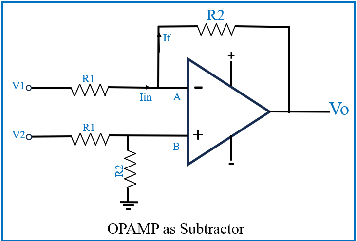
In this subtractor circuit, V1 is connected to the inverting terminal through resistor R1, and V2 is connected to the non-inverting terminal via another R1. Resistor R2 is placed between the non-inverting terminal and ground, while the feedback resistor R2 connects the output (Vo) to the inverting terminal. The circuit outputs the difference between V1 and V2, scaled by the feedback network, with the inverting terminal at virtual ground for accurate subtraction.

Because of the high input impedance, the current entering the OPAMP is zero.

Therefore, potential at point B is
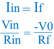
VB = [R2/(R1+R2)]V2 and Iin = If
(V1-VA)/R1 = (VA-Vo)/R2

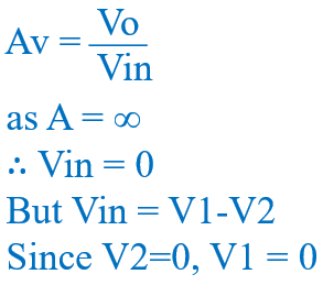
As the open loop gain of the OPAMP is very high
From virtual ground concept,
Vo = A(VA-VB) where A → VA = VB

(V1/R1)-[R2/(R1+R2)]x(V2/R1) = [R2/(R1+R2)]x(V2/R2) - (Vo/R2)
(V1/R1)-[R2/(R1+R2)]x(V2/R1) -[R2/(R1+R2)]x(V2/R2) =-(Vo/R2)
(V1/R1)-[V2/(R1+R2)]x[(R2/R1)+1]= -(Vo/R2)
(V1/R1)-[V2/(R1+R2)]x[(R1+R2)/R1]= -(Vo/R2)
(V1/R1)-(V2/R1)= - (Vo/R2)
Vo=-(R2/R1)x(V1-V2)
Vo=(R2/R1)x(V2-V1)
If R1=R2 then
Vo= V2-V1

In this way, an OPAMP configured as a subtractor effectively computes the difference between two input signals, providing a useful tool for applications in signal processing and measurement.

3] OPAMP as a Differentiator

An operational amplifier (op-amp) can be configured as a differentiator, producing an output voltage that is proportional to the rate of change (derivative) of the input signal. This property makes differentiators particularly useful in applications such as waveform shaping, signal analysis, and control systems.

In a basic differentiator circuit, the input signal is applied to a capacitor connected to the inverting input of the op-amp. A feedback resistor is connected from the output to the inverting input. The non-inverting input is typically grounded. This arrangement allows the circuit to respond to rapid changes in the input signal.

Capacitor (C): The capacitor passes changes in voltage but blocks steady-state (DC) signals.
Resistor (R): The feedback resistor determines the output voltage based on the rate of change of the input voltage.

The differentiator circuit is sensitive to high-frequency components due to the nature of the capacitor. As frequency increases, the capacitive reactance decreases, allowing higher rates of change in the input voltage to result in larger output responses.

Derivation:
Here, we know If = -Iin

This states that the feedback current through the resistor R is equal in magnitude and opposite in direction to the input current through the capacitor.

(Vo/R) = -C (dVin/dt)
Vo =-RC (dVin/dt)
When RC =1 then
Vo = =-(dVin/dt)

In this way, an op-amp configured as a differentiator effectively amplifies the rate of change of the input signal, producing an output that is sensitive to high-frequency components. This configuration is vital for various signal processing applications, allowing for the shaping and analysis of waveforms based on their instantaneous rates of change.

4] OPAMP as an Integrator

An op-amp can be configured as an integrator, where the output voltage is proportional to the integral of the input signal over time. This configuration is particularly useful in applications such as analog computation, signal processing, and control systems.
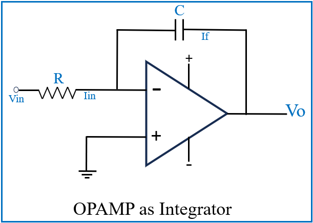
In an integrator circuit, the input signal is applied to the inverting terminal of the op-amp through a resistor, while a capacitor is connected from the output to the inverting terminal. The non-inverting terminal is typically grounded.

Derivation:
Here, we know If = -Iin

If =-(Vin/R)

But if If is capacitive current it is CdVo/dt
Equating the two current expressions gives
CdVo/dt = -(Vin/R)
Rearranging the equation:
dVo = -(Vin dt/RC)

Integrating both sides

∫dVo = -1/RC ∫ Vin dt
Vo = -1/RC ∫ Vin dt
if RC = 1 then


Vo = -∫Vin dt

In this way, an op-amp configured as an integrator effectively converts a time-varying input signal into a corresponding output voltage that represents the accumulated value of the input over time. This configuration is crucial in various applications, facilitating advanced signal processing and control in electronic circuits.

5] OPAMP as Voltage follower (Buffer)

A voltage follower, also known as a buffer amplifier, is a configuration of an op-amp that provides a unity gain (gain of 1) while isolating the input from the output. In this configuration, the output voltage directly follows the input voltage, making it useful for impedance matching and signal buffering.
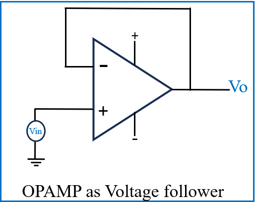
In a voltage follower circuit, the op-amp is connected in a non-inverting configuration. The output is connected directly to the inverting terminal, creating a feedback loop that maintains the output voltage equal to the input voltage.

Here,

Vo = (1+ Rf/Rin)Vin
Vo = (1+ 0) Vin
Vo=Vin
The voltage gain Av is therefore:
Av=Vo/Vin =1

In this way, a voltage follower effectively provides signal isolation and prevents loading effects on the previous stage while maintaining the same voltage level. This makes it an essential component in various applications, such as interfacing between circuits with different impedances.

Conclusion

Operational amplifiers (OPAMPs) are powerful components that play a crucial role in analog electronics. Their ability to perform various mathematical operations — such as addition, subtraction, integration, and differentiation — makes them essential building blocks in signal processing, control systems, and instrumentation. Whether used as summing amplifiers, subtractors, differentiators, integrators, or voltage followers, OPAMPs provide versatility, precision, and reliability. Understanding these fundamental applications allows engineers to design and optimize circuits for a wide range of real-world scenarios, from audio mixers to sensor signal conditioning. Mastering these configurations lays the foundation for more advanced applications in both analog and digital systems.

October 6, 2024

Analog Electronics Chapter 3: Exploring Key Characteristics of Operational Amplifiers (OPAMPs)

Operational amplifiers (OPAMPs) have several important characteristics that make them vital components in analog circuits. These properties directly influence how OPAMPs behave in various applications, from signal amplification to filtering and computation.

1] Open loop gain:

The open loop gain of an OPAMP is its differential gain under conditions where no feedback is provided. Ideally its value is infinite. i.e.

Av = Vo/Vid and Vid<<<Vo

With infinite open-loop gain, even the smallest difference between the input terminals would be greatly amplified, making the OPAMP highly sensitive to input signals.

2] Closed loop gain:

The overall gain of OPAMP with feedback is known as closed loop gain(Acl). OPAMP is generallt used with feedback,the gain is adjusted by feedback resistor which has a range of 10³ or 10⁵. Closed-loop gain is predictable and stable, making the OPAMP useful for a wide range of controlled amplification tasks.

3] Input impedance:

OPAMPs input impedance Zin is the impedance looking into its input terminals. As shown in below figure, it determine how much current it takes from the input voltage. Infinite input impedance ensures that no current flows into the amplifier input terminals.
Zin= Vin/Iin = infinite

4] Output Impedance:

It is the resistance looking from the output. It determines how much maximum current it gives without drop in output voltage. if Z0 = 0 ohms full amplified voltage Av * Vid appears at the output. Zero output impedance allows the OPAMP to provide maximum power to the load. This means that the output voltage remains constant, irrespective of the connected load, ensuring efficient power transfer. Ideally Zo=Vo/Io = 0

5] Infinite bandwidth:

Bandwidth is the range of frequency for which OPAMP works with maximum gain. Ideally, OPAMPs bandwidth is infinite practically it is in MHz. An infinite bandwidth means that the OPAMP can amplify signals of any frequency without attenuation. This characteristic allows the OPAMP to operate across a wide range of frequencies, making it versatile for different applications.

6] Input bias current:

Input bias current is the small amount of current that flows into the input terminals of an OPAMP to operate the internal transistors. In an ideal OPAMP, this current should be zero, meaning no current is drawn from the signal source. However, in real-world OPAMPs, a small bias current is necessary for the transistors at the input stage to function.

This bias current typically ranges from picoamperes (for FET-based OPAMPs) to nanoamperes (for bipolar OPAMPs). Although small, input bias current can cause voltage drops across resistors in the circuit, introducing errors in sensitive or high-precision applications, such as instrumentation amplifiers or integrators.

To minimize the impact of input bias current, designers often use matched resistors or compensate for it with external circuits, especially when precision and accuracy are paramount.

7] Input offset current:

Input offset current is the difference between the bias currents flowing into the two input terminals of an operational amplifier. Ideally, these bias currents should be equal, but in real-world OPAMPs, slight mismatches occur due to internal transistor imbalances.

This difference, though typically small (in the nanoampere range), can lead to inaccuracies in the output, especially in high-precision applications. It can cause an offset in the output voltage, even when the input voltage is zero. In sensitive circuits, input offset current can be reduced by using precision OPAMPs or compensating with external resistors.

8] Input Offset Voltage

Input offset voltage is the small voltage that must be applied between the inverting and non-inverting terminals to force the output to zero when it should ideally be zero. In an ideal OPAMP, this voltage is zero, meaning both inputs would perfectly match in the absence of any input signal.

In practical OPAMPs, due to imperfections in the internal components, a small offset voltage (in the millivolt or microvolt range) is required to balance the internal circuitry. This can lead to errors in precision applications, especially when amplifying small signals. High-quality OPAMPs typically have lower input offset voltages, and external trimming techniques or offset adjustment pins are often used to minimize this effect.

9] Slew Rate

Slew rate defines how quickly the output of an OPAMP can change in response to a change in the input signal. It is typically expressed in volts per microsecond (V/µs). A higher slew rate means the OPAMP can respond to rapid changes in the input signal without distortion.

10] Drift

Drift refers to the slow, unintended changes in OPAMP parameters (like input offset voltage and bias currents) over time or with changes in temperature. Low drift is crucial for applications that require long-term stability and precision.

11] CMRR:

CMRR (Common-Mode Rejection Ratio) is a measure of how well an operational amplifier (OPAMP) can reject common-mode signals, i.e., signals that appear simultaneously and in phase at both the inverting and non-inverting input terminals. Ideally, an OPAMP should amplify only the differential signal (the voltage difference between the two input terminals) and completely reject common-mode signals, like noise or interference.

Formula:
CMRR is expressed as the ratio of the differential gain A diff to the common-mode gain A cm, usually in decibels (dB):

Differential Gain Adiff : The gain of the OPAMP when amplifying the difference between the inverting and non-inverting inputs.
Common-Mode Gain Acm : The gain of the OPAMP when amplifying signals that are common to both inputs.
A higher CMRR indicates better performance in rejecting noise or unwanted signals that are common to both inputs, which is especially important in noisy environments or when dealing with small differential signals in the presence of large common-mode signals.

12] PSRR:

PSRR (Power Supply Rejection Ratio) measures how well an operational amplifier rejects variations in its power supply voltage. It quantifies the ability of the OPAMP to maintain a consistent output even when there are fluctuations or noise in the supply voltage. Ideally, variations in the power supply should have no effect on the OPAMP’s output, but in reality, some changes in output do occur due to power supply fluctuations.

Formula:
PSRR is also expressed in decibels (dB) as the ratio of the change in power supply voltage (ΔVsupply) to the resulting change in output voltage (ΔVout):

A high PSRR value indicates that the OPAMP can effectively suppress changes in the output due to variations in the power supply, making it more resilient to supply noise or instability.
PSRR is typically high at low frequencies but can degrade at higher frequencies, which means high-frequency noise from the power supply could still affect the output.

13] Frequency Response

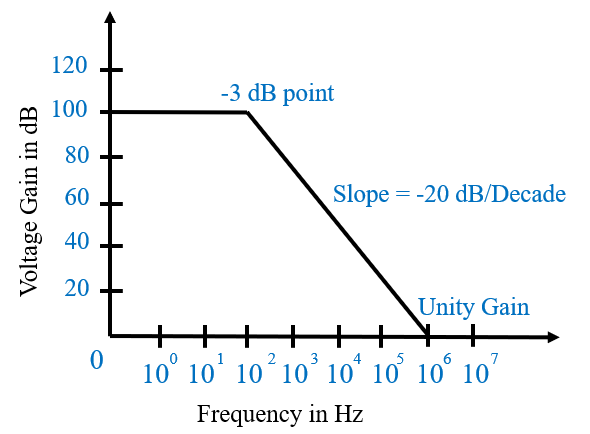
The frequency response of an OPAMP describes how its gain varies with frequency. While OPAMPs can ideally amplify signals across all frequencies, real-world devices have a limited bandwidth where gain starts to decrease at higher frequencies. Understanding the frequency response is essential when designing circuits for high-speed or high-frequency applications. Below diagram represents the frequency response of OPAMP:
Let’s break down the key elements:

Flat Region (Low Frequencies):

At lower frequencies, the op-amp maintains a constant voltage gain (around 100 dB in this case). This is the open-loop gain of the op-amp.
-3 dB Point:

This point marks the beginning of the roll-off. It is the frequency where the gain drops by 3 dB from the maximum value. This corresponds to the op-amp’s bandwidth limit for higher precision.
Roll-off Slope (-20 dB/decade):

Beyond the -3 dB point, the gain decreases at a rate of -20 dB/decade. This means the gain drops by 20 dB for every tenfold increase in frequency. This roll-off is typical of a single-pole system, which is common for op-amps.
Unity Gain Frequency:

The point where the gain reaches 0 dB (unity gain). It indicates the highest frequency at which the op-amp can amplify without any gain (effectively acting as a buffer).

Conclusion

Understanding these key characteristics of operational amplifiers is crucial for designing effective analog circuits. From gain control and input impedance to slew rate and frequency response, these parameters shape how OPAMPs function across various applications in signal processing, control systems, and instrumentation.

October 2, 2024

Analog Electronics Chapter 2: Exploring Inverting and Non-Inverting OPAMPs

OPAMP as Inverting Amplifier

The inverting amplifier configuration is one of the most common and widely used configurations of an operational amplifier (OPAMP). In this setup, the input signal is applied to the inverting terminal, and the non-inverting terminal is grounded. Let’s break down the diagram and understand the workings of this circuit in detail, along with formulas, the concept of virtual ground, and key characteristics.

Circuit Overview

Inverting Terminal (-): The input voltage (Vin) is applied to the inverting terminal through a resistor Rin.
Non-Inverting Terminal (+): The non-inverting terminal is connected to ground, creating a reference point for the operational amplifier.
Feedback Resistor (Rf): A resistor is placed between the output (Vo) and the inverting terminal, allowing feedback of a portion of the output signal back to the input.
Virtual Ground: Even though the non-inverting terminal is connected to ground (0V), due to the nature of the OPAMP, the voltage at the inverting terminal also behaves as if it were at 0V, creating what is called a “virtual ground.” This is explained in detail later.

Working of the Inverting Amplifier
The inverting amplifier works based on two fundamental principles of the operational amplifier in closed-loop configuration:

1. Virtual Ground
The concept of virtual ground is central to understanding how an inverting OPAMP functions. Here’s a detailed explanation:

In an ideal OPAMP, the open-loop gain is extremely high, often considered infinite. This causes the difference between the inverting and non-inverting inputs to be nearly zero when the OPAMP is in closed-loop configuration (with feedback).
If the non-inverting terminal is connected to ground (0V), the inverting terminal will also be at 0V, even though it’s not physically connected to ground. This is because the OPAMP works to maintain this condition to ensure the input difference is nearly zero.
Therefore, the inverting terminal behaves as if it were at ground potential (0V), although no direct connection to ground exists. This behavior is referred to as a virtual ground.
It’s important to note that while the voltage at the inverting terminal is 0V, current still flows through the resistors Rin and Rf, allowing the circuit to function properly.

2. No Current Flow Into Input Terminals: The OPAMP’s input impedance is extremely high, meaning that no current flows into the inverting or non-inverting terminals of the OPAMP. This leads to the assumption that all the input current through Rin must flow through the feedback resistor Rf.

Gain Formula for the Inverting Amplifier
To derive the gain, we apply Kirchhoff’s Current Law (KCL) at the inverting node.

1. The current through Rin due to Vin:

2. The current through the feedback resistor Rf:

Since no current flows into the OPAMP’s inverting terminal, the input current Iin must equal the feedback current If:

Rearranging to solve for the output voltage Vo:

Thus, the gain of the inverting amplifier is:

The negative sign indicates that the output is inverted with respect to the input signal, meaning it is 180 degrees out of phase.

This configuration is widely used in applications like signal conditioning, audio amplification, and analog computation due to its predictable gain and phase inversion properties.

OPAMP as Non-Inverting Amplifier

The non-inverting amplifier is another fundamental configuration of an operational amplifier (OPAMP), where the input signal is applied to the non-inverting terminal, resulting in an output signal that is in phase with the input. Unlike the inverting amplifier, the output is not inverted, and the gain can be easily controlled through external resistors.

Circuit Overview
In the non-inverting amplifier circuit:

Non-Inverting Terminal (+): The input voltage (Vin) is applied directly to the non-inverting terminal.
Inverting Terminal (-): The inverting terminal is connected to a voltage divider consisting of two resistors (Rf and R1), which provide feedback to the inverting terminal.
Feedback Resistor (Rf): The feedback resistor connects the output (Vo) back to the inverting terminal to control the gain of the amplifier.
Ground: The other end of R1 is grounded, which helps to set the gain along with Rf.

Working of the Non-Inverting Amplifier
The non-inverting amplifier operates based on the following principles of the operational amplifier:

1. Virtual Short: In an ideal OPAMP with infinite gain, the difference in voltage between the inverting and non-inverting terminals is nearly zero. Therefore, the voltage at the inverting terminal is almost equal to the input voltage Vin, a condition known as a virtual short.

V2 ≈ V1 = Vin

2. No Current Flow Into Input Terminals: Since the input impedance of an ideal OPAMP is extremely high, no current flows into either the inverting or non-inverting terminals. All the current flows through the resistors R1 and Rf.

Gain Formula for the Non-Inverting Amplifier
To derive the gain of the non-inverting amplifier, we can use the concept of a voltage divider across R1 and Rf.

The voltage at the inverting terminal (V1) is a fraction of the output voltage (Vo) based on the voltage divider formed by R1 and Rf:

Since V1 ≈ Vin due to the virtual short, we can equate V1 to Vin:

Rearranging to solve for Vo:

Thus, the gain of the non-inverting amplifier is:

In this case, the gain is always positive and greater than or equal to 1. The output signal is in phase with the input, unlike the inverting configuration where the output is inverted.

This configuration is widely used in applications like voltage buffering, signal amplification, and interfacing with high-impedance sources, thanks to its high input impedance and ability to preserve the phase of the input signal.

Conclusion

In this chapter, we examined two essential operational amplifier configurations: the inverting and non-inverting amplifiers. The inverting amplifier is known for inverting the input signal with a predictable gain, making it suitable for applications like audio processing. Its operation relies on the concept of virtual ground.

Conversely, the non-inverting amplifier preserves the phase of the input signal while allowing for adjustable gain, making it ideal for voltage buffering and interfacing with high-impedance sources.

Mastering these configurations is crucial for advancing in analog electronics and designing effective circuits.

Explore Our Topics!

Check out the extensive list of topics we discuss:  Communication Protocols: -  USB   - RS232   -  Ethernet   -  AMBA Protocol: APB, AHB and...