Showing posts with label silicon. Show all posts

November 20, 2024

A Day in the Life of a Semiconductor: From Silicon to Superpower

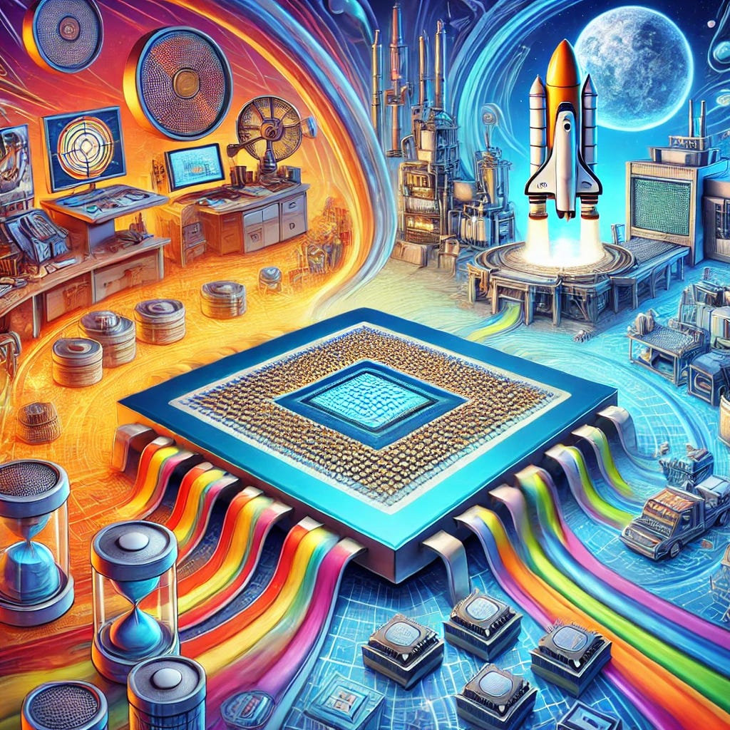
Ever wondered what it’s like to be a semiconductor? Well, buckle up! Imagine waking up every morning in a lab with machines buzzing around you, ready to transform you into the brainpower behind everything from your smartphone to your self-driving car. Sounds exciting, right? Let’s take a quirky, fun-filled journey through a typical day in the life of a semiconductor, from dawn to dusk.

6:00 AM: Waking Up in the Lab

As the sun peeks through the high-tech windows, I’m already busy being prepared for my day. I’m a piece of silicon — just a tiny speck in the vast world of electronics. But don’t let my size fool you; I’m about to be turned into a microchip that powers some of the most complex and important technologies in the world.

I start my day on a giant wafer — yep, that’s my bed for now. Think of it as a shiny pancake that’s waiting to be transformed. But before I get into all the action, I have to endure hours of photolithography and etching. Fun fact: I don’t get a say in where I’m etched, but I’m cool with it. I’m designed to make a difference.

8:00 AM: The “Spa” Treatment

After the initial prep, it’s time for my first “spa treatment” — or, as the engineers like to call it, the cleaning process. I’m scrubbed, polished, and inspected to make sure I’m flawless. All those little imperfections — oh, they have no place here. I’ve got to be as smooth and perfect as a freshly baked cookie (minus the crumbs, of course).

I can feel the heat, the energy flowing through me as I get charged up. It’s not just a beauty treatment, it’s about getting me ready to be used in the most powerful machines on Earth. My pores — aka transistors — are etched to make sure I’m ready to carry out those complicated logic operations that humans love me for.

10:00 AM: Becoming a Transistor

Now comes the fun part — becoming transistors! You may have heard of them before. They’re the tiny switches that control the flow of electricity inside a chip. Every semiconductor like me has billions of them, and we work as a team to process data, compute, and keep everything running smoothly.

There’s a lot of excitement in the air. Each of us transistors is like a little worker in a massive factory, passing information back and forth. But don’t worry — there’s no chaos. It’s all organized. Just imagine a group of ants working together in perfect harmony, only we’re not ants. We’re much, much faster.

1:00 PM: Time to Meet the Chip Designers

After all that hard work, it’s time to meet the chip designers. This is the moment where all my carefully etched patterns and transistors are brought together into one beautiful, high-functioning microchip. It’s kind of like being in an assembly line, but with a lot more thoughtfulness. The designers make sure my architecture is perfect. My layout has to be just right: fast, efficient, and ready to take on the world.

There’s a lot of attention to detail — every little wire, every little connection needs to be in place for me to work flawlessly. Honestly, it’s a bit like playing Tetris, but with billions of tiny components instead of colorful blocks. The designers look happy, which means they’re pleased with how I’m shaping up. I’m almost ready for the big leagues!

3:00 PM: Enter the Testing Lab

After I’m assembled into my final form (a microchip, in case you were wondering), it’s time to go through some stress testing. This is where the fun begins! Think of it as an intense bootcamp for me.

The engineers run me through a battery of tests: electrical stress tests, thermal tests, and even mechanical tests. Will I survive the extreme conditions of space travel? Can I withstand the heat of a powerful computer? These tests will make sure I’m strong enough to handle anything. Honestly, I feel like I’m being prepped for my own action movie. The Semiconductor Chronicles: Rise of the Chips — anyone? 😜

5:00 PM: Packing Up for the Big Journey

After surviving the testing phase, I’m packed and shipped off to my new home. Whether I’m destined to be inside your smartphone, a supercomputer, or even a spaceship, this is the part of the day when I get to leave the lab and join the real world. It’s both exciting and nerve-wracking.

Will I become the powerhouse behind a groundbreaking technology? Or will I end up in a lesser-known device that simply sends emails and plays music? Either way, I’m ready. This is my destiny!

8:00 PM: A Well-Deserved Rest

At last, I’m installed into my final device. The user switches it on, and BOOM — I’m doing what I was born to do: powering everything behind the scenes. I might not get the credit for all the cool things my host device does, but I know that without me, none of it would work.

For now, it’s time for me to rest. Well, kind of. I’ll be on standby, waiting for the next task. After all, a semiconductor’s work is never truly done. From here, I’ll be activated and deactivated thousands of times, providing the power and processing abilities that make the world go round.

The Next Morning: Rinse and Repeat

And so, the cycle continues. Every day is a new adventure for a semiconductor like me. Sure, I may be small, but the impact I have on the world is anything but. From powering devices to enabling technology that can change the course of human history, I’m proud to be at the heart of it all.

So, the next time you power on your device, take a moment to appreciate the tiny chip inside. You may not see me, but I’m always there — doing my part to make the world a little smarter, faster, and more connected.

Liked this fun journey through the life of a semiconductor? Share it with your friends who love tech, and stay tuned for more quirky posts on electronics and technology!

Explore Our Topics!

Check out the extensive list of topics we discuss:  Communication Protocols: -  USB   - RS232   -  Ethernet   -  AMBA Protocol: APB, AHB and...