Showing posts with label full adder. Show all posts

June 16, 2024

Understanding the Half Adder: A Fundamental Building Block in Digital Electronics.

In the realm of digital electronics, the ability to perform arithmetic operations is crucial. Among the fundamental components that enable these operations are adders, with the Half Adder being one of the simplest yet essential types. This blog will explore the Half Adder, its components, functionality, and significance in digital circuit design.

What is a Half Adder?

A Half Adder is a digital circuit that performs the addition of two single-bit binary numbers. It produces two outputs: a sum bit and a carry bit. The simplicity of the Half Adder makes it a fundamental building block for more complex arithmetic circuits, such as Full Adders and arithmetic logic units (ALUs).

Theoretical Background

Before delving into the Half Adder, it is essential to understand the basics of binary addition. In binary arithmetic:

  1. 0 + 0 = 0
  2. 0 + 1 = 1
  3. 1 + 0 = 1
  4. 1 + 1 = 10 (which is 0 with a carry of 1)

Components of a Half Adder

A Half Adder consists of two primary components:

  • XOR Gate: Produces the sum bit.
  • AND Gate: Produces the carry bit.

The logical expressions for the outputs are:

  • Sum (S) = A XOR B
  • Carry © = A AND B

Circuit Diagram

The circuit diagram of a Half Adder is straightforward, with an XOR gate and an AND gate connected as shown below:

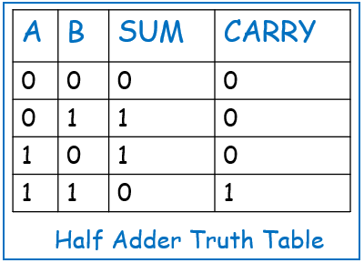
Truth Table

The truth table below illustrates how the Half Adder operates for all possible input combinations:
Applications of Half Adder

Half Adders are fundamental components in digital electronics and have several applications, primarily in the construction of more complex arithmetic circuits. Here are some key applications:

  1. Building Full Adders: Half Adders are used to construct Full Adders, which can add binary numbers of more than one bit. A Full Adder adds three bits (two significant bits and a carry bit) and produces a sum and a carry bit. By cascading multiple Full Adders (which themselves are built from Half Adders), you can create circuits capable of adding multi-bit binary numbers. This forms the basis of ripple-carry adders and other multi-bit adder architectures.
  2. Arithmetic Logic Units (ALUs): Half Adders are integral to the design of ALUs, which perform a variety of arithmetic and logical operations in microprocessors and digital systems. ALUs use Half Adders and Full Adders to perform binary addition, which is a fundamental operation in computing.
  3. Digital Signal Processing (DSP): Efficient Data Manipulation: In DSP applications, Half Adders are used for efficient data manipulation and processing tasks that require binary addition. Simple binary calculators use Half Adders to perform basic addition operations. They serve as the foundational units that enable binary addition in these devices.
  4. Memory Address Calculation: In memory systems, Half Adders help in the calculation of memory addresses during read and write operations, ensuring data is stored and retrieved correctly.
  5. Digital Counters: Half Adders are used in digital counters, where they help in performing the increment operations necessary for counting sequences.
  6. Encoders and Decoders: In encoders and decoders, Half Adders assist in converting data between different binary codes, which is essential in various digital communication and storage systems.
  7. Error Detection and Correction: Half Adders are used in generating checksums for error detection and correction in data transmission. They help in adding binary values to produce checksums that verify data integrity.

Conclusion

The Half Adder is a fundamental component in digital electronics, serving as a building block for more complex arithmetic circuits. Its simplicity and essential role in binary addition make it a critical topic for anyone studying digital logic design. Understanding the functionality, applications, and implementation of the Half Adder provides a solid foundation for exploring more advanced digital circuits.

For those interested in practical implementations, I have detailed blogs on how to implement a Half Adder using both VHDL and Verilog on Xilinx Vivado. Click on the links below to explore the full implementations and testbench code:

Stay tuned for more detailed blogs on combinational circuits and other key topics in digital electronics.

June 11, 2024

Understanding the Full Adder: A Key Component in Digital Electronics

In the realm of digital electronics, the ability to perform arithmetic operations efficiently is crucial. Among the fundamental components enabling these operations are adders, with the Full Adder standing as a significant advancement from the Half Adder. This blog will explore the Full Adder, its components, functionality, and its crucial role in digital circuit design.

What is a Full Adder?

A Full Adder is a digital circuit that adds three single-bit binary numbers: A, B, and an input carry, C_in. It produces two outputs: a sum bit (S) and an output carry bit (C_out). Unlike the Half Adder, which can only add two bits without considering a carry, the Full Adder can add three bits and account for a carry input.

Theoretical Background

Before delving into the Full Adder, it is essential to understand the basics of binary addition. In binary arithmetic:

  1. 0 + 0 = 0
  2. 0 + 1 = 1
  3. 1 + 0 = 1
  4. 1 + 1 = 10 (which is 0 with a carry of 1)

Components of a Full Adder

A Full Adder consists of three primary components:

  • XOR Gate: Generates the sum bit (S), considering all inputs A, B, and C_in.
  • AND Gate: Produces the carry bit (C_out), considering all possible combinations of A, B, and C_in.
  • OR Gate: Combines the carry outputs from the AND gate and the XOR gate to produce the final carry output.

The logical expressions for the outputs are:

  • Sum (S) = A XOR B XOR C_in
  • Carry out (C_out) = (A AND B) OR (C_in AND (A XOR B))

Circuit Diagram

The circuit diagram of a Full Adder is more complex than a Half Adder, incorporating XOR, AND, and OR gates as shown below:

Truth Table

The truth table below illustrates how the Full Adder operates for all possible input combinations of A, B, and C_in:

If we want to design the Full Adder using half adders, the block diagram and circuit diagram for it will be as follows:

Applications of Full Adder

Full Adders are crucial components in digital electronics and have several applications, primarily in the construction of more complex arithmetic circuits. Here are some key applications:

  1. Cascade to Build Multi-bit Adders: Full Adders are used to construct adders capable of adding multi-bit binary numbers. This forms the basis of ripple-carry adders and other multi-bit adder architectures.
  2. Arithmetic Logic Units (ALUs): Integral to ALU design, Full Adders perform binary addition operations as part of microprocessors and digital systems.
  3. Digital Signal Processing (DSP): Used in DSP applications for efficient data manipulation tasks requiring binary addition.
  4. Binary Calculators: Foundational units in simple binary calculators to perform basic arithmetic operations.
  5. Memory Address Calculation: Aid in calculating memory addresses during read and write operations in memory systems.
  6. Digital Counters: Assist in increment operations for counting sequences in digital counters.
  7. Encoders and Decoders: Used to convert data between different binary codes, essential in digital communication and storage systems.
  8. Checksum Generators: Generate checksums for error detection and correction in data transmission to ensure data integrity.
  9. Logic Circuit Design: Serve as teaching tools in educational settings to illustrate the principles of digital logic and binary addition.

Conclusion

The Full Adder represents a significant advancement from the Half Adder in digital electronics, crucial for constructing more complex arithmetic circuits. Its ability to handle three input bits and manage carry operations makes it an essential component in binary arithmetic and digital system design. Understanding the functionality, applications, and implementation of the Full Adder provides a robust foundation for exploring advanced digital circuits.

For practical implementations and further exploration, check out detailed blogs on how to implement a Full Adder using VHDL and Verilog on Xilinx Vivado. Click on the links below to delve into full implementations and testbench code:

  1. Implementing Full Adder using VHDL
  2. Implementing Full Adder using Verilog

Stay tuned for more detailed blogs on combinational circuits and other essential topics in digital electronics.

Explore Our Topics!

Check out the extensive list of topics we discuss:  Communication Protocols: -  USB   - RS232   -  Ethernet   -  AMBA Protocol: APB, AHB and...