Showing posts with label esim. Show all posts

June 7, 2023

Step-by-step guide on how to implement a Vending Machine Controller using VLSI.

  • In this project, I have designed and implemented Vending Machine Controller using VHDL using Quartus Prime and Modelsim software.
  • To explore the project you can git clone using this command: git clone Github

Table of Contents:

  1. INTRODUCTION
    1.1 FSM (Finite State Machine)
  2. RELATED WORK
  3. IMPLEMENTATION OF VENDING MACHINE
  4. DESIGN METHODOLOGY
  5. SIMULATION RESULTS
  6. CONCLUSION
  7. REFERENCES

1. INTRODUCTION

Vending Machine is an electronic machine used to dispense a product to a consumer after a prescribed amount of money has been put into the machine. Considering the current situation, the three most important things we need when we are outside are sanitizer, tissue paper, and paper soap for cleanliness and sanity purposes. So, we are designing a Vending Machine Controller using VHDL for sanitizer, tissue paper, and paper soap. This machine can be used at various places like railway stations, food stalls, etc.

The FPGA based Vending machines are reprogrammable, flexible, and more advantageous in terms of speed, response, and power consumption. FPGA based machines can be reprogrammed without the need to change the whole architecture when enhancing the model of the machine. Microcontrollers sequentially execute all operations whereas an FPGA is a field programmable gate array that will execute all your operations in a parallel fashion.

1.1 FSM (Finite State Machine) [2] [3]

In a Finite State Machine, the circuit’s output is defined in a different set of states i.e. each output is a state. A State Register to hold the state of the machine and a next state logic to decode the next state. An output register defines the output of the machine. In FSM based machines the hardware gets reduced as in this the whole algorithm can be explained in one process.

Two types of State machines are:

MEALY Machine: In this machine model, the output depends on the present state as well as on the input. The MEALY machine model is shown in figure 1.

Figure 1: MEALY Machine Model

MOORE Machine: In the Moore machine model the output only depends on the present state. The MOORE machine model is shown in figure 2.

Figure 2: MOORE Machine Model

2. RELATED WORK

Various researches have been carried out in order to design the Vending Machines. A few of them are discussed here as Ana Monga, Balwinder Singh [1] propose a vending machine for designing multi select machines using Finite State Machine Model with Auto-Billing Features. In this paper, the process of four states (user Selection, Waiting for money insertion, product delivery, and servicing) has been modeled using MEALY Machine Model. The proposed model is tested using Spartan 3 development board and its performance is compared with CMOS based machine. The various methods of designing VHDL based machines are discussed in [2], [3], and [4]. In the paper [5] Design and Implementation of an automatic Beverages Vending Machine and its performance evaluation using Xilinx ISE and Cadence, the design and implementation of an automatic beverages vending machine using FSM as this technique is compared with previous ones used in vending machine design and the whole design is verified using Xilinx ISE simulator 13.1 and the implemented using Virtex 5 XC5VLX50T FPGA board and its physical design has performed using Cadence Encounter and evaluated its optimized parameters.

3. IMPLEMENTATION OF VENDING MACHINE
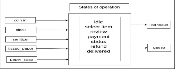
Figure 3: Block Diagram

Vending machine for Sanitizertissue paper, and paper soap is designed using Quartus Prime Software. It can be deployed in the form of VHDL code, RTL view, and output waveform. The system will accept 3 inputs sanitizer, tissue paper, and paper soap, and will give the total cost. The complete cycle will run around 6 states idle, select item, review, payment status, refund, and delivered. If the amount is more than cost price change is returned and if the amount is less than the cost price complete amount is returned with no delivery.

4. DESIGN METHODOLOGY
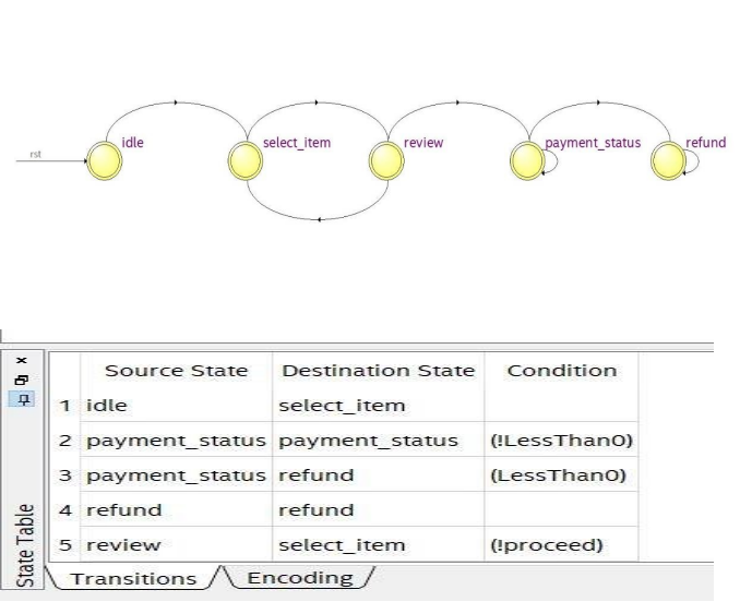
The code will accept three inputs and the system will run around 5 states idle, select_item, review, payment_status, and refund. Initially, it will be at an idle state and after each clock cycle, it will change its state. The next state will be select_item state where you can individually select from the given inputs and then it will go to review state where it will give you the total amount so you can check whether it is correct or not. If the total amount is correct it will go to payment_status state where you can enter the amount and it will then go in the refund based on comparing it with the total amount. If the cost entered is less than the total cost then it will refund the complete entered amount and will give no delivery similarly if the cost entered is more than the total cost it will refund the change and give the delivery.

Description of states
The selection of products and all the states is shown below:
when idle => p_s <= select_item ;
when select_item =>
temp := (10 *sanitizer + 5 *tissue_paper + 1 *paper_soap );
total <= temp ;
p_s <= review ;
when review =>
if (proceed =’1') then
p_s <= payment_status;
elsif(proceed = ‘0’ ) then
p_s <= select_item ; end if ;
when payment_status =>
if (temp <= coin_in) then
delivered <= ‘1’ ;
p_s <= refund ;
elsif(temp > coin_in ) then
delivered <= ‘0’ ;
coin_out <= coin_in ;
p_s <= payment_status;
end if ;
when refund => coin_out <= coin_in-temp;

Similarly, we can add other products also.

5. SIMULATION RESULTS

The Simulation is done using Modelsim software. Initially, the reset is set to 0 and the clock signal is given and then the state changes from idle to select_item state where I have selected 5 sanitizers, 5 tissue paper, and 5 paper soap. According to the pre-defined formula, the total amount must be 80 and we have received the same in the review state then we set to proceed to 1 and state changes to payment state where I have considered three different cases.

  1. In the first state, I have set the coin into 70 which is less than the total amount so according to the code it must return the whole amount i.e. 70 in the refund section and the delivered signal must be 0 and we have successfully got the same results.
  2. In the second state, the coin in input is set to 100 which is more than the total amount hence it must return 20 in the refund section and the delivered signal must become 1 and we have successfully got the results of the 2nd case correctly
  3. Now, in the third state, I have considered an idle state where we have entered the correct coin in the amount which is 80, and hence it should return 0 in the refund section and the delivered signal must be 1, here also we have successfully got the correct results.
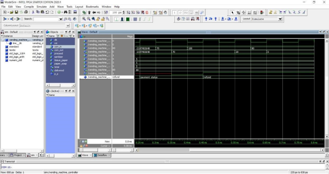
OUTPUT WAVEFORM

The below figure shows the complete RTL view:
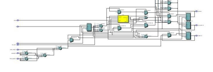
Figure 4: RTL View

I have divided the RTL view into two sections in the below figure as input and output part of the RTL view.
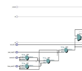
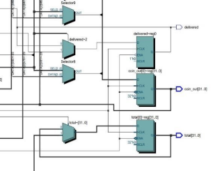
Figure 5: Input Section
Figure 6: Output Section

6. CONCLUSION

The above system can be implemented using any FPGA Development Board where you can select the items using on-off buttons and similarly display the amount and its status using LCD or OLED. State machine based vending Systems increases productivity reduces system development cost and accelerates the time to market. We can easily increase the number of inputs and also add different features to the system.

7. REFERENCES

  1. Ana Monga, Balwinder Singh “Finite State Machine based Vending Machine Controller with Auto-Billing Features” International Journal of VLSI design & Communication Systems (VLSICS) Vol.3, №2, April 2012.
  2. Xilinx Inc., Spartan 3 Datasheet: http://www.xilinx.com.
  3. Bhaskar “VHDL primer” Second Edition,
  4. C. J Clement Singh, K Senthil Kumar, Jayanto Gope, Suman Basu & Subir Kumar Sarkar (2007) “Single Electron Device based Automatic Tea Vending Machine*” proceedings of International Conference on Information and Communication Technology in Electrical Sciences (ICTES 2007),* pp 891–896.
  5. V.V.S.Vijay Krishna, A. Monisha, Sk.Sadulla, J. Prathiba “Design and Implementation of an automatic Beverages Vending Machine and its performance evaluation using Xilinx ISE and Cadence” IEEE — 31661

Like, Share and Follow me if you like my content.
Thank You.

January 6, 2023

Step-by-step guide on how to design and implement a Full adder using CMOS and sky130nm PDK.

  • The purpose of this project is to design a CMOS FULL ADDER using an Opensource EDA Tool called eSim, an Opensource Spice Simulator called ngspice, and Sky130 PDK. 
  • To explore the project, you can git clone using the command: git clone Github.

Table of Contents:

  1. INTRODUCTION
  2. INSTALLATION OF TOOLS
  3. CIRCUIT DESIGN
    3.1. REFERENCE CIRCUIT DIAGRAM
    3.2. REFERENCE CIRCUIT WAVEFORM
  4. IMPLEMENTATION
  5. REFERENCE

1. INTRODUCTION

In this project, I am going to Design and Implement a FULL ADDER using CMOS Technology and I will also implement it using sky130nm technology. Design and Implementation will be done using esim and ngspice software. Full Adder is the digital circuit that will add 3 inputs and give 2 outputs. 3 inputs are A, B, C, and outputs are SUM, CARRY. Full Adder will do binary addition of A, B, and C and will give the sum of 3 inputs at SUM output and carry bit at CARRY output. We can verify the output using Circuit Waveforms. This complete design and implementation is done using VLSI technology which has features such as high speed, low power, low cost, and small size.

2. INSTALLATION OF TOOLS

esim:

esim is an open-source EDA tool used for circuit design and simulation. Using esim we can draw a circuit using Kicad, generate netlist and simulate using Ngspice.

For more information: https://esim.fossee.in/home

Ngspice:

ngspice is the open-source spice simulator for electric and electronic circuits. We can design circuits using JFET, MOSFET, and passive elements like resistors, capacitors, etc.

For more information: http://ngspice.sourceforge.net

Sky130nm PDK:

The SkyWater Open Source PDK is a collaboration between Google and SkyWater Technology Foundry to provide a fully open source Process Design Kit and related resources, which can be used to create manufacturable designs at SkyWater’s facility.

For more information: https://www.layouteditor.org/schematiceditor/libraries/skywater

The Download links for the above software are:

esim: https://esim.fossee.in/downloads

Ngspice: https://sourceforge.net/projects/ngspice/files/

Sky130 pdk: https://static.fossee.in/esim/installation-files/sky130_fd_pr.zip

Follow these steps for Sky130 download and implementaion:

  1. Download sky130 from this link mentioned above and unzip it.
  2. Save the .cir.out file in the sky_fd_pr folder as .cir file.
  3. Open with notepad and add the path .lib “models/sky130.lib.spice” tt at the top.
  4. Replace with CMOSP, mos_p with sky130_fd_pr_pfet_01v8 and CMOSN, mos_n with sky130_fd_pr_nfet_01v8.
  5. To replace the inductor, capacitor, resistor do it this way, for Ex: L1 out gnd 1m by x1 out gnd mid 0 sky130_fd_pr__ind_03_90.

Note: For more details go to the cells folder in sky_fd_pr.

Open the specific component folder which you want to use.

Then open the test folder and check the SPICE file.

The SPICE file is an example of the implementation of that component.

You will get to know how to use the component in your ckt.

  1. Now Run the circuit with ngspice.

To Run the ckt using ngspice:

  1. Right click on the .cir file.
  2. Click on Open With.
  3. Browse for the ngspice.
  4. If ngspice is not present scroll down click on More Apps.
  5. Go to the FOSSEE folder search for Ngspice and Run it.

3. CIRCUIT DESIGN

Full Adder is a digital circuit that will add 3 binary inputs and will give 2 outputs namely SUM and CARRY. The 3 inputs are A, B, and C and outputs are SUM and CARRY. As we have 3 inputs we will have 8 input combinations. Using circuit design rules of CMOS we will design the circuit in such a way that the addition of 3 inputs will occur at SUM output and the carry bit will occur at CARRY output. While designing we have used a total of 28 Transistors. Full Adder using CMOS will be designed using 2 parts: PMOS (pull-up lattice) and NMOS (pull-down lattice). PMOS circuit is connected to supply voltage VDD and NMOS circuit is connected to ground GND. We will implement this circuit design using sky130nm technology. In the Circuit Waveform, we will verify the above implementation using clock pulse. In the output, we will give different input combinations through clock pulse and verify the logic using the output waveform.

3.1 REFERENCE CIRCUIT DIAGRAM

3.2 REFERENCE CIRCUIT WAVEFORM

4. IMPLEMENTATION

Now, we will design the complete circuit using our reference circuit diagram with PMOS logic above and NMOS logic below. After connecting the complete we will get a circuit like below:

Label each and every component and port and check electrical rule checking and generate netlist file using spice and make changes in the netlist to add sky130 models. The netlist generated initially is as shown below:

C:\SPB_Data\eSim-Workspace\Full_Adder\abc.cir
EESchema Netlist Version 1.1 (Spice format) creation date: 2/8/2022 1:04:47 PM
To exclude a component from the Spice Netlist add [Spice_Netlist_Enabled] user FIELD set to: N
To reorder the component spice node sequence add [Spice_Node_Sequence] user FIELD and define sequence: 2,1,0
Sheet Name: / M1 /vdd /vin_a Net-M1-Pad3 /vdd mosfet_p
M2 /vdd /vin_a Net-M2-Pad3 /vdd mosfet_p
M3 /vdd /vin_b Net-M2-Pad3 /vdd mosfet_p
M4 /vdd /vin_c Net-M4-Pad3 /vdd mosfet_p
M5 /vdd /vin_a Net-M4-Pad3 /vdd mosfet_p
M6 /vdd /vin_b Net-M4-Pad3 /vdd mosfet_p
M7 Net-M1-Pad3 /vin_b Net-M14-Pad2 /vdd mosfet_p
M8 Net-M2-Pad3 /vin_c Net-M14-Pad2 /vdd mosfet_p
M9 Net-M4-Pad3 Net-M14-Pad2 Net-M12-Pad3 /vdd mosfet_p
M10 /vdd /vin_a Net-M10-Pad3 /vdd mosfet_p
M11 Net-M10-Pad3 /vin_b Net-M11-Pad3 /vdd mosfet_p
M12 Net-M11-Pad3 /vin_c Net-M12-Pad3 /vdd mosfet_p
M13 /vdd Net-M12-Pad3 /sum /vdd mosfet_p
M28 /sum Net-M12-Pad3 GND GND mosfet_n
M21 Net-M14-Pad2 /vin_b Net-M15-Pad1 GND mosfet_n
M15 Net-M15-Pad1 /vin_a GND GND mosfet_n
M16 Net-M16-Pad1 /vin_a GND GND mosfet_n
M17 Net-M16-Pad1 /vin_a GND GND mosfet_n
M18 Net-M18-Pad1 /vin_c GND GND mosfet_n
M22 Net-M14-Pad2 /vin_c Net-M16-Pad1 GND mosfet_n
M19 Net-M18-Pad1 /vin_a GND GND mosfet_n
M23 Net-M12-Pad3 Net-M14-Pad2 Net-M18-Pad1 GND mosfet_n
M20 Net-M18-Pad1 /vin_b GND GND mosfet_n
M26 Net-M12-Pad3 /vin_c Net-M25-Pad1 GND mosfet_n
M25 Net-M25-Pad1 /vin_b Net-M24-Pad1 GND mosfet_n
M24 Net-M24-Pad1 /vin_a GND GND mosfet_n
M27 /carry Net-M14-Pad2 GND GND mosfet_n
M14 /vdd Net-M14-Pad2 /carry /vdd mosfet_p
U1 /vdd /vin_a /vin_b /vin_c /sum /carry PORT
.end

The netlist after making sky130 models syntax changes is as shown below:

c:\spb_data\esim-workspace\full_adder\full_adder.cir
.lib “sky130_fd_pr/models/sky130.lib.spice” tt
xM1 vdd vin_a Net-M1-Pad3 vdd sky130_fd_pr__pfet_01v8 w=1 l=0.5
xM7 Net-M1-Pad3 vin_b Net-M14-Pad2 vdd sky130_fd_pr__pfet_01v8 w=1 l=0.5
xM2 vdd vin_a Net-M2-Pad3 vdd sky130_fd_pr__pfet_01v8 w=1 l=0.5
xM3 vdd vin_b Net-M2-Pad3 vdd sky130_fd_pr__pfet_01v8 w=1 l=0.5
xM8 Net-M2-Pad3 vin_c Net-M14-Pad2 vdd sky130_fd_pr__pfet_01v8 w=1 l=0.5
xM4 vdd vin_c Net-M4-Pad3 vdd sky130_fd_pr__pfet_01v8 w=1 l=0.5
xM5 vdd vin_a Net-M4-Pad3 vdd sky130_fd_pr__pfet_01v8 w=1 l=0.5
xM6 vdd vin_b Net-M4-Pad3 vdd sky130_fd_pr__pfet_01v8 w=1 l=0.5
xM9 Net-M4-Pad3 Net-M14-Pad2 Net-M12-Pad3 vdd sky130_fd_pr__pfet_01v8 w=1 l=0.5
xM21 Net-M14-Pad2 vin_b Net-M15-Pad1 GND sky130_fd_pr__nfet_01v8 w=0.42 l=0.5
xM15 Net-M15-Pad1 vin_a GND GND sky130_fd_pr__nfet_01v8 w=0.42 l=0.5
xM22 Net-M14-Pad2 vin_c Net-M16-Pad1 GND sky130_fd_pr__nfet_01v8 w=0.42 l=0.5
xM16 Net-M16-Pad1 vin_a GND GND sky130_fd_pr__nfet_01v8 w=0.42 l=0.5
xM17 Net-M16-Pad1 vin_b GND GND sky130_fd_pr__nfet_01v8 w=0.42 l=0.5
xM23 Net-M12-Pad3 Net-M14-Pad2 Net-M18-Pad1 GND sky130_fd_pr__nfet_01v8 w=0.42 l=0.5
xM18 Net-M18-Pad1 vin_c GND GND sky130_fd_pr__nfet_01v8 w=0.42 l=0.5
xM19 Net-M18-Pad1 vin_a GND GND sky130_fd_pr__nfet_01v8 w=0.42 l=0.5
xM20 Net-M18-Pad1 vin_b GND GND sky130_fd_pr__nfet_01v8 w=0.42 l=0.5
xM10 vdd vin_a Net-M10-Pad3 vdd sky130_fd_pr__pfet_01v8 w=1 l=0.5
xM11 Net-M10-Pad3 vin_b Net-M11-Pad3 vdd sky130_fd_pr__pfet_01v8 w=1 l=0.5
xM12 Net-M11-Pad3 vin_c Net-M12-Pad3 vdd sky130_fd_pr__pfet_01v8 w=1 l=0.5
xM26 Net-M12-Pad3 vin_c Net-M25-Pad1 GND sky130_fd_pr__nfet_01v8 w=0.42 l=0.5
xM25 Net-M25-Pad1 vin_b Net-M24-Pad1 GND sky130_fd_pr__nfet_01v8 w=0.42 l=0.5
xM24 Net-M24-Pad1 vin_a GND GND sky130_fd_pr__nfet_01v8 w=0.42 l=0.5
xM13 vdd Net-M12-Pad3 sum vdd sky130_fd_pr__pfet_01v8 w=1 l=0.5
xM28 sum Net-M12-Pad3 GND GND sky130_fd_pr__nfet_01v8 w=0.42 l=0.5
xM14 vdd Net-M14-Pad2 carry vdd sky130_fd_pr__pfet_01v8 w=1 l=0.5
xM27 carry Net-M14-Pad2 GND GND sky130_fd_pr__nfet_01v8 w=0.42 l=0.5
Vdd vdd 0 3.3
Vd0 vin_a 0 pulse(0 2.2 0us 0s 0s 20us 40us)
Vd1 vin_b 0 pulse(0 2.2 5us 0s 0s 20us 40us)
Vd2 vin_c 0 pulse(0 2.2 15us 0s 0s 20us 40us)
.tran 0.1us 60us
.control
run
plot V(carry) V(sum) +4 V(vin_c) +8 V(vin_b) +12 V(vin_a)+15
.endc
.end

Note: sky130_fr_pd file for sky130 model must be present on the same file as .cir.out.

Truth Table for Full Adder using CMOS is as shown below:

Now, run the .cir.out file using ngspice and we will get the circuit waveforms as follows:

From the above waveform, we can verify the truth table for Full Adder using CMOS.

5. REFERENCES:

[1]N. Zhuang and H. Wu, “A new design of the CMOS full adder,” IEEE Journal of Solid-State Circuits, vol. 27, №5, pp. 840–844, May 1992.

[2]N. H. E. Weste and K. Eshraghian, “Principles of CMOS VLSI design,” Addison Wesley, 1993.

Like, Share and Follow me if you like my content.
Thank You.

Explore Our Topics!

Check out the extensive list of topics we discuss:  Communication Protocols: -  USB   - RS232   -  Ethernet   -  AMBA Protocol: APB, AHB and...