Signal Integrity
Let’s break down the term “Signal Integrity”:
What is a Signal?
A signal can be defined as information used for communication between two points, usually in the form of a wave or pulse. In analog form, it can be a wave, and in digital form, it will be in the form of a state 1 (high state) or state 0 (low state). The figure below shows a simple example of a signal in digital form:

What is Integrity?
Integrity can be defined simply as completeness or lack of distortion. It can also be defined as the ability to transmit a signal over time without losing any information or experiencing distortion.
So, Signal integrity can be defined as the ability of a signal to transmit information from one point to another without losing signal quality or information, while also resisting the effects of high-frequency electromagnetic interference from nearby signals.
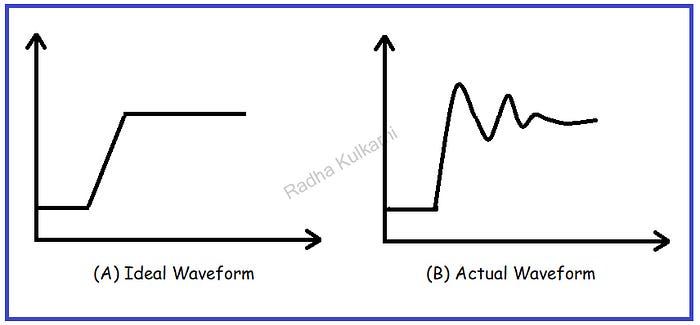
- In digital design, signal integrity primarily focuses on two things:
- Ensuring that the signal arrives at the receiving end within the desired timeframe.
- Ensuring that the signal is in the same condition as it was at the transmitting end.
- Factors which affect signal integrity are:
- Antenna Effect: Refers to the undesired pickup of noise or interference by long metal traces acting as antennas.
- Crosstalk: Unwanted coupling of signals between adjacent nets.
- IR drop: Voltage drop due to resistance of the conductors.
- Ground Bounce: Caused by simultaneous switching noise affecting the ground potential.
- Electromigration: Gradual movement of metal atoms in a conductor due to high current density.
- What are Eye diagrams?
An eye diagram is a tool used in digital systems to check signal quality. It shows the rising and falling edges of a bitstream in a time domain trace. Engineers use eye diagrams to detect and fix issues that affect data communication and performance, such as crosstalk, EMI, signal loss, and bit-error rate. Creating an eye diagram requires simulating millions of bits and matching the impedance of the transmitter, interconnect, and receiver to eliminate reflections.
Now let us discuss what is Crosstalk??
Crosstalk is a phenomenon that occurs in digital systems when the transmission of signals on one net produces undesired effects on adjacent nets. Crosstalk may lead to step up and hold time violations.
To provide a clear illustration of crosstalk, consider the following example:
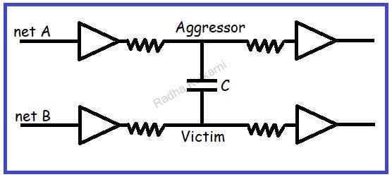
Consider, 2 adjacent nets net A and net B with some dielectric between them.
Aggressor net: This refers to the net that switches and causes undesired effects on adjacent nets.
Victim net: This refers to the net that is affected by the undesired effects caused by the agressor net.
In this example, net A is the aggressor net and net B is the victim net. So, due to some reason the aggressor net will cause an effect such as voltage spikes on the Victim net and distorts its output causing degradation in performance and reliability in ICs.
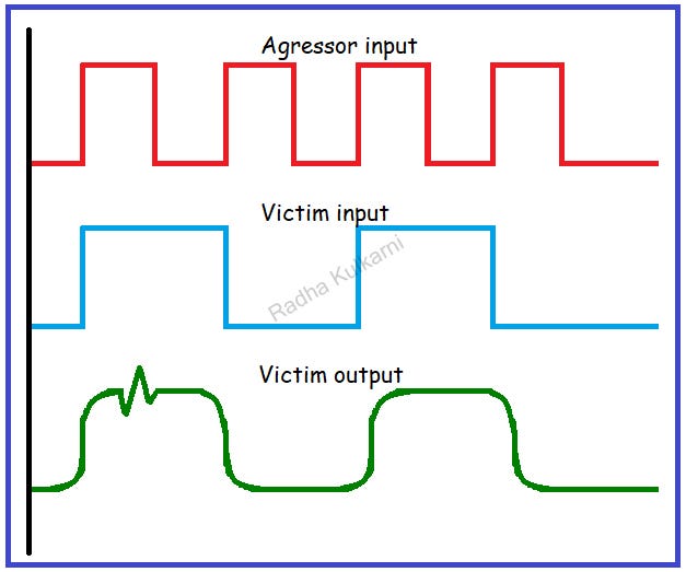
- Crosstalk can have two primary effects on electronic signals:
- Crosstalk noise: During signal transmission, the aggressor net can cause a noise bump or glitch on the victim net. This can negatively impact the functionality and timing of the device.
- Crosstalk delay: This refers to the delay in the victim net output that results from the effect of the aggressor net on it. The degree of delay depends on the switching direction of the aggressor and victim nets.
- When considering crosstalk in the data path, the following scenarios may occur:
- If both the aggressor and victim nets switch in the same direction, the victim transition may occur too quickly, causing data to arrive early and potentially resulting in a hold violation. This scenario is good for setup but bad for hold.
- If both the aggressor and victim nets switch in the opposite direction, the victim transition may occur more slowly, increasing the delay and potentially resulting in a setup violation. This scenario is good for hold but bad for setup.
- When considering crosstalk in the clock path, the following scenarios may occur:
- If both the aggressor and victim nets switch in the same direction, the victim transition may occur too quickly, causing data to arrive early and potentially resulting in a setup violation. This scenario is good for hold but bad for setup.
- If both the aggressor and victim nets switch in the opposite direction, the victim transition may occur more slowly, increasing the delay and potentially resulting in a hold violation. This scenario is good for setup but bad for hold.
- What is crosstalk glitch??
The sudden glitch that occurs in the victim net as a result of crosstalk from the aggressor net is known as a crosstalk glitch. This glitch can be of two types:
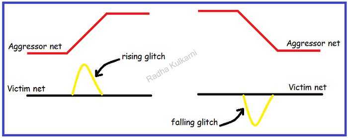
- Rising Glitch: If the aggressor net switches from low to high and victim net is in a constant logic 0 then due to the crosstalk from agressor net the victim net gets a sudden rising glitch.
- Falling Glitch: If the aggressor net switches from high to low and victim net is in a constant logic 1 then due to the crosstalk from agressor net the victim net gets a sudden falling glitch.
- What is Glitch Height and its Effects?
To understand the concept of glitch height, let’s take an example of a CMOS inverter. The diagram below illustrates a CMOS inverter and its transfer characteristics:
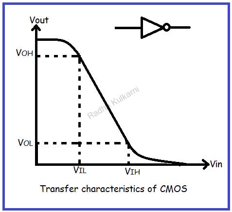
In this diagram:
- VOH represents the range of output voltage that is considered as logic 1 or high.
- VOL represents the range of output voltage that is considered as logic 0.
- VIL represents the range of input voltage that is considered as logic 0 or low.
- VIH represents the range of input voltage that is considered as logic 1.
The output of an inverter cell may be high as long as the input stays below the maximum value of VIL, and the output of the inverter cell may be low as long as the input stays above the minimum value of VIH.
Now, when we plot the graph for voltages (output low, VOL; input low, VIL; output high, VOH; input high, VIH) against time, we obtain the following graph:
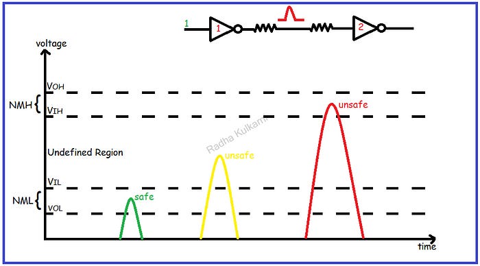
In the graph, the region between VOL and VIL is known as the noise margin low (NML), and the region between VOH and VIH is known as the noise margin high (NMH). The region between VIL and VIH is considered as the undefined region.
The noise margin refers to the amount of noise that a CMOS circuit can tolerate without affecting its operation.
Here, two CMOS inverters are connected in series, and a logic 1 (high) is applied as Vin.
If, due to crosstalk or other factors, the value of Vin after the first inverting operation falls between VOL and VIL, i.e., in the noise margin low region, the output is considered as safe, and a logic 0 (low) is passed to inverter 2.
Similarly, if the value of Vin falls between VIH and VOH, i.e., in the noise margin high region, the output is considered as unsafe, and a logic 1 (high) is fed to inverter 2.
If the value of Vin falls between NMH and NML, i.e., in the undefined region, it is considered as unsafe because Vin can take any value, i.e., logic 1 or 0 (high or low).
- The height of crosstalk glitches depends on several factors:
1) Coupling Capacitance:
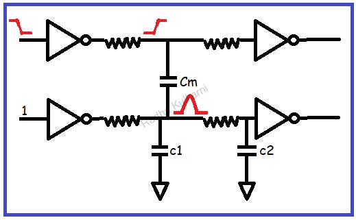
The glitch height is influenced by the coupling capacitance between two nets. In the diagram below, Cm represents the mutual capacitance. The mutual capacitance depends on the distance between the two nets. Thus, a smaller distance between the aggressor net and the victim net results in a larger coupling capacitance and, consequently, a larger glitch height.

2) Aggressor Drive Strength:
A higher drive strength at the aggressor net results in a faster slew rate, leading to a higher crosstalk glitch height.
3) Victim Drive Strength:
Similarly, a higher drive strength at the victim net results in a lower crosstalk glitch height.
- Now, let’s consider a few cases where both the aggressor net and victim net are transitioning at the same time:
- Aggressor net is switching from low to high and victim net is switching from high to low at the same time. Due to the coupling capacitance between the aggressor and victim nets, the switching in the aggressor net can cause a bump or affect the transition time, resulting in an increased delay in the victim net. If the initial delay in the cell is D, then due to crosstalk, the final delay will be D + Δ.
- If both the aggressor net and victim net are switching from low to high, then due to crosstalk, the transitioning time for the victim net will decrease, leading to a reduced delay and transitioning slope. If the initial delay in the cell is D, then due to crosstalk, the final delay will be D — Δ.
Both of these cases can be summarized in the figure below.
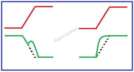
Hence, the change in the delay of the victim cell due to crosstalk from the aggressor net is called “Crosstalk Delta Delay”.
- What happens when there are multiple aggressors?
When multiple aggressor nets switch at the same time, the crosstalk coupling effect on the victim net is compounded due to the presence of multiple aggressors. To determine the bump height on the victim net, the bump heights caused by all aggressor nets are added together.
- Methods to prevent Crosstalk:
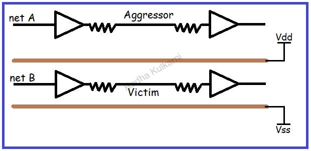
1) Shielding:
In shielding, the victim nets are covered with wider nets called shielding nets, as shown in the diagram below. These shielding nets are generally much wider nets than the normal routing nets. These shielding nets are directly connected to a strong VDD or VSS. This protects the victim net from the effects of crosstalk.
2) Spacing:
Increasing the spacing between two nets can decrease the crosstalk effect. Let’s see how:
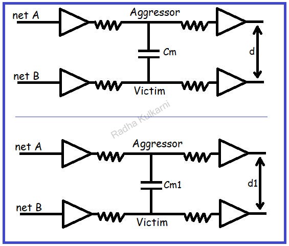
Initially, if the distance between the two nets is d and the capacitance is Cm, increasing the distance to d1 and capacitance to Cm1 will decrease the mutual capacitance between the aggressor and victim nets. As capacitance is inversely proportional to the distance and directly proportional to the glitch height h, increasing the distance (d) will decrease the capacitance (Cm), and in turn, reduce the crosstalk glitch height.
3) Increasing the drive strength of the victim net.
4) Decreasing the drive strength of the aggressor net.
5) Fast slew rate: Increasing the slew rate makes the net less susceptible to crosstalk and reduces the likelihood of crosstalk effects.
In conclusion, signal integrity and crosstalk effects are significant factors that impact the performance, reliability, and functionality of ICs. Proper understanding, management, and mitigation of signal integrity and crosstalk effects are critical for designing robust and reliable ICs in modern electronic systems.