Showing posts with label NOR Gate. Show all posts

April 11, 2024

Mastering Verilog: Implementing Logic Gates.

Welcome to the world of digital design! In this blog post, we’ll dive into Verilog code examples for essential logic gates used in digital circuits. Understanding how to implement these gates is foundational for building complex digital systems.

For a detailed insight into how these logic gates operate, including their truth tables, click on the link provided below:
Logic Gates

Below, you’ll find Verilog code implementations for various logic gates using two different methods:
1. Behavioral Modeling: Describes the logic behavior using `always @(*)` blocks.
2. Dataflow Modeling: Describes the logic using continuous assignments (`assign`).

1. AND Gate

Behavioral Modeling:

module AND_Gate(input wire a, input wire b, output reg y);
always @(*) begin
y = a & b;
end
endmodule

Dataflow Modeling:

module AND_Gate(input wire a, input wire b, output wire y);
assign y = a & b;
endmodule

2. OR Gate

Behavioral Modeling:

module OR_Gate(input wire a, input wire b, output reg y);
always @(*) begin
y = a | b;
end
endmodule

Dataflow Modeling:

module OR_Gate(input wire a, input wire b, output wire y);
assign y = a | b;
endmodule

3. NAND Gate

Behavioral Modeling:

module NAND_Gate(input wire a, input wire b, output reg y);
always @(*) begin
y = ~(a & b);
end
endmodule

Dataflow Modeling:

module NAND_Gate(input wire a, input wire b, output wire y);
assign y = ~(a & b);
endmodule

4. NOR Gate

Behavioral Modeling:

module NOR_Gate(input wire a, input wire b, output reg y);
always @(*) begin
y = ~(a | b);
end
endmodule

Dataflow Modeling:

module NOR_Gate(input wire a, input wire b, output wire y);
assign y = ~(a | b);
endmodule

5. XOR Gate

Behavioral Modeling:

module XOR_Gate(input wire a, input wire b, output reg y);
always @(*) begin
y = a ^ b;
end
endmodule

Dataflow Modeling:

module XOR_Gate(input wire a, input wire b, output wire y);
assign y = a ^ b;
endmodule

6. XNOR Gate

Behavioral Modeling:

module XNOR_Gate(input wire a, input wire b, output reg y);
always @(*) begin
y = ~(a ^ b);
end
endmodule

Dataflow Modeling:

module XNOR_Gate(input wire a, input wire b, output wire y);
assign y = ~(a ^ b);
endmodule

Conclusion

These Verilog code snippets demonstrate two ways of implementing logic gates:

- Behavioral Modeling is more abstract and suitable for complex logic, using `always` blocks to describe how the logic should behave.
- Dataflow Modeling is closer to the gate-level, where continuous assignments (`assign`) directly describe how the inputs connect to the outputs.

Experiment with both methods to understand their behavior and use them as building blocks for creating sophisticated digital designs.
Happy Coding!

April 4, 2024

From Theory to Practice: CMOS Logic Circuit Design Rules Made Easy with Examples.

In the realm of VLSI circuit design, understanding CMOS (Complementary Metal-Oxide-Semiconductor) logic circuits is crucial. CMOS circuits are built using two types of transistors: nMOS (negative-channel Metal-Oxide-Semiconductor) and pMOS (positive-channel Metal-Oxide-Semiconductor). Let’s delve into the intricacies of CMOS logic design and explore how theory translates into practical circuitry.

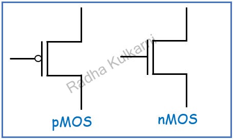
  • Working Principles of nMOS and pMOS Transistors:
  1. nMOS: When the gate voltage is “0,” the nMOS transistor is OFF, acting as an open circuit. Conversely, with a gate voltage of “1,” it turns ON, behaving like a short circuit.
  2. pMOS: With a gate voltage of “0,” the pMOS transistor is ON, acting as a short circuit. When the gate voltage is “1,” it becomes OFF, akin to an open circuit.
  • Structure of CMOS Circuits:
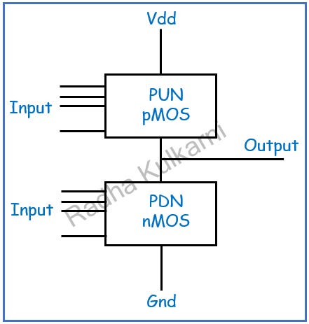
  1. CMOS circuits consist of a pull-up network made of pMOS transistors and a pull-down network made of nMOS transistors.
  2. The pull-up network connects to Vdd (the supply voltage) while the pull-down network connects to GND (ground).
  3. The output is derived from the connection between the pull-up and pull-down networks.
  4. pMOS transistors are efficient at passing logic high signals, while nMOS transistors excel at passing logic low signals.
  5. Due to the inherent inverting nature of CMOS, an inverter circuit is typically added at the output to obtain a non-inverted signal.
  • Basic Logic Circuit Rules:

In CMOS logic design, two fundamental operations are performed:

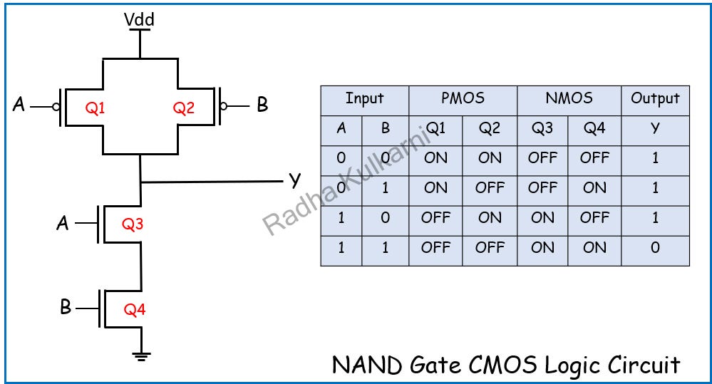
  1. The “ . “ operation, also known as the AND operation, involves connecting pMOS transistors in parallel and nMOS transistors in series.
  2. The “ + “ operation, or OR operation, connects nMOS transistors in parallel and pMOS transistors in series.
  • Examples:
  1. NAND Gate

2. NOR Gate

“Stay tuned for more examples and insights into CMOS logic design as we continue to explore the fascinating world of VLSI circuitry.”

In conclusion, understanding the intricacies of CMOS logic circuits, including the working principles of nMOS and pMOS transistors, the structure of CMOS circuits, and the basic logic circuit rules, is essential for anyone delving into VLSI circuit design. By grasping how theory translates into practical circuitry, we gain insights into creating efficient and robust digital systems.
Thank you for joining us on this exploration of CMOS logic design, and we look forward to sharing more knowledge and insights with you in the future.

February 4, 2024

Unveiling the World of Logic Gates: The Building Blocks of Digital Circuits


  • Logic gates serve as fundamental building blocks that execute logical operations on binary inputs, resulting in binary outputs. These gates form the foundation of digital circuits, playing a pivotal role in the processing and manipulation of digital information.
  • Truth table provides a systematic representation of potential input combinations alongside their respective outputs for a given logic gate or logical expression. In this table, each row signifies a distinct set of input values, with the corresponding output determined by the behavior of the logic gate.
  • Following are the types of Logic gates:
  1. AND
  2. OR
  3. NOT
  4. NOR
  5. NAND
  6. XOR
  7. XNOR
  • Let’s delve into the specifics of each logic gate:

1] AND Gate:

An AND gate features a single output and multiple inputs. When all inputs are high (1), the output is high (1). The Boolean logic is expressed as Y = A.B for two inputs, A and B. The AND gate is represented by the following symbol and truth table:

2] OR Gate:

The OR gate accepts two or more inputs and produces one output. If at least one input is high (1), the output is high (1). The mathematical expression for a two-input OR gate is Y = A + B. The OR gate symbolizes its logic, where the output is high when any input is high. The OR gate is represented by the following symbol and truth table:

3] NOT Gate:

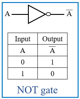
The NOT gate is a single-input, single-output gate. It produces the inverse of its input, and its Boolean equation is Y = A’. It is also known as an inverter. The NOT gate is represented by the following symbol and truth table:

4] NOR Gate:

A NOR gate is formed by combining an OR gate followed by a NOT gate. The output is high only when all inputs are low (0). The Boolean statement for the NOR gate is Y=(A+B)’ if there are two inputs A and B. It can serve as a universal gate for implementing OR, AND, and NOT.

5] NAND Gate:

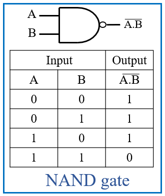
A NAND gate is essentially a Not gate followed by an AND gate. The output is low only when none of the inputs is low (0). If there are two inputs A and B, the Boolean expression for the NAND gate is Y=(A.B)’. The NAND gate is known as a universal gate because it may be used to implement the AND, OR, and NOT gates.

6] XOR Gate:

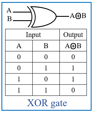
The Exclusive-OR or ‘Ex-OR’ gate is a digital logic gate that accepts more than two inputs but only outputs one value. If any of the inputs is 1 the output of the XOR Gate is 1. If both inputs are ‘1’ the output is ‘0’ If both inputs are ‘0’ the output is ‘0’.
The Boolean equation for the XOR gate is Y=A’.B+A.B’ if there are two inputs A and B. The XOR gate is represented by the following symbol and truth table:

7] XNOR:

The Exclusive-NOR or ‘EX-NOR’ gate is a digital logic gate that accepts more than two inputs but only outputs one. If both inputs are ‘1’ the output of the XNOR Gate is ‘1’ If both inputs are ‘0’ the output is ‘1’ If one of the inputs is 0’ the output is ‘0’. If there are two inputs A and B, then the XNOR gate’s Boolean equation is: Y=A.B+A’B’. The truth table shows that its outputs are based on NOR gate logic. The XNOR gate is represented by the following symbol and truth table:

Exploring the intricate world of logic gates has unveiled the fundamental building blocks of digital circuits. We’ve navigated through the functions of AND, OR, NOT, NOR, NAND, XOR, and XNOR gates, unraveling their symbolic representations, Boolean equations, and truth tables. Understanding these essential components is key to mastering digital circuit design. As we close this exploration, let the knowledge of logic gates empower your journey into the realm of digital electronics and circuitry.

Like, Share and Follow me if you like my content.
Thank You.

Explore Our Topics!

Check out the extensive list of topics we discuss:  Communication Protocols: -  USB   - RS232   -  Ethernet   -  AMBA Protocol: APB, AHB and...