Very Large Scale Integration (VLSI) is a process that integrates millions of transistors onto a single chip, revolutionizing the field of electronics. This intricate journey involves several critical steps, collectively known as the VLSI design flow. In this blog, we will explore each phase of this fascinating process, from initial specifications to the final testing and packaging.
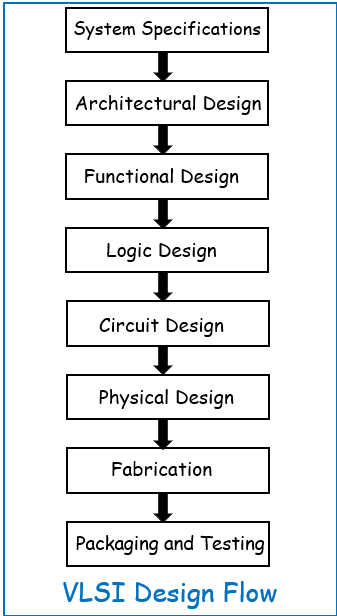
The below diagram shows the Design Flow in VLSI.

1. System Specifications
The journey begins with defining the system specifications. This phase sets the foundation for the entire design process by outlining performance targets, functionality requirements, physical dimensions, fabrication technology, and design techniques.
- Performance: Speed, power consumption, and efficiency.
- Functionality: Desired operations and features.
- Physical Dimensions: Chip size constraints.
- Fabrication Technology: Choice of technology node (e.g., 5nm, 7nm).
- Design Techniques: Methodologies and tools to be used.
2. Architectural Design
Next, we move to architectural design, where the high-level structure of the chip is defined. This includes:
- Module Definition: Defining modules in terms of inputs, outputs, and functionality.
- ALUs and Floating Point Units: Determining the number and types.
- Pipelines and Caches: Structure and sizes.
3. Functional Design
In functional design, we delve into detailed analysis and estimation of area, power, and performance parameters for each unit. This phase typically results in timing diagrams that illustrate how data moves through the system.
4. Logic Design
Logic design translates the functional design into a detailed logic representation.
- Control Flow: Managing data and instruction flow.
- Word Width and Register Allocation: Defining bit-widths and register usage.
- Arithmetic and Logic Operations: Specifying operations and their implementations.
The outcome is an RTL (Register Transfer Level) description using HDLs like VHDL or Verilog.
5. Circuit Design
In this stage, the RTL description is converted into a circuit representation. Key considerations include:
- Speed and Power Requirements: Ensuring the circuit meets performance goals.
- Circuit Simulation: Verifying correctness and timing.
The result is a netlist, a detailed circuit diagram showing all components and their connections, often generated automatically using logic synthesis tools.
6. Physical Design
Physical design is perhaps the most complex phase, where the netlist is transformed into a geometric representation known as a layout.
- Geometric Representation: Converting logic components into geometric shapes.
- Layered Connections: Representing interconnections as lines across multiple layers.
7. Fabrication
Once the layout is verified, it’s time for fabrication. This involves:
- Photolithographic Masks: Creating masks for each layer.
- Wafer Processing: Growing silicon crystals, slicing wafers, and processing them according to the masks.
8. Packaging and Testing
The final step involves cutting the wafer into individual chips, packaging them, and conducting rigorous testing to ensure they meet all specifications.
Conclusion
The VLSI design flow is a complex and meticulously detailed process that transforms a concept into a functioning silicon chip. Each phase requires careful planning, precise execution, and thorough verification to ensure the final product performs as intended.