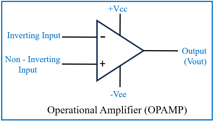
Operational amplifiers (OPAMPs) have several important characteristics that make them vital components in analog circuits. These properties directly influence how OPAMPs behave in various applications, from signal amplification to filtering and computation.
1] Open loop gain:
The open loop gain of an OPAMP is its differential gain under conditions where no feedback is provided. Ideally its value is infinite. i.e.
Av = Vo/Vid and Vid<<<Vo
With infinite open-loop gain, even the smallest difference between the input terminals would be greatly amplified, making the OPAMP highly sensitive to input signals.
2] Closed loop gain:
The overall gain of OPAMP with feedback is known as closed loop gain(Acl). OPAMP is generallt used with feedback,the gain is adjusted by feedback resistor which has a range of 10³ or 10⁵. Closed-loop gain is predictable and stable, making the OPAMP useful for a wide range of controlled amplification tasks.
3] Input impedance:

OPAMPs input impedance Zin is the impedance looking into its input terminals. As shown in below figure, it determine how much current it takes from the input voltage. Infinite input impedance ensures that no current flows into the amplifier input terminals.
Zin= Vin/Iin = infinite
4] Output Impedance:
It is the resistance looking from the output. It determines how much maximum current it gives without drop in output voltage. if Z0 = 0 ohms full amplified voltage Av * Vid appears at the output. Zero output impedance allows the OPAMP to provide maximum power to the load. This means that the output voltage remains constant, irrespective of the connected load, ensuring efficient power transfer. Ideally Zo=Vo/Io = 0
5] Infinite bandwidth:
Bandwidth is the range of frequency for which OPAMP works with maximum gain. Ideally, OPAMPs bandwidth is infinite practically it is in MHz. An infinite bandwidth means that the OPAMP can amplify signals of any frequency without attenuation. This characteristic allows the OPAMP to operate across a wide range of frequencies, making it versatile for different applications.
6] Input bias current:
Input bias current is the small amount of current that flows into the input terminals of an OPAMP to operate the internal transistors. In an ideal OPAMP, this current should be zero, meaning no current is drawn from the signal source. However, in real-world OPAMPs, a small bias current is necessary for the transistors at the input stage to function.
This bias current typically ranges from picoamperes (for FET-based OPAMPs) to nanoamperes (for bipolar OPAMPs). Although small, input bias current can cause voltage drops across resistors in the circuit, introducing errors in sensitive or high-precision applications, such as instrumentation amplifiers or integrators.
To minimize the impact of input bias current, designers often use matched resistors or compensate for it with external circuits, especially when precision and accuracy are paramount.
7] Input offset current:
Input offset current is the difference between the bias currents flowing into the two input terminals of an operational amplifier. Ideally, these bias currents should be equal, but in real-world OPAMPs, slight mismatches occur due to internal transistor imbalances.
This difference, though typically small (in the nanoampere range), can lead to inaccuracies in the output, especially in high-precision applications. It can cause an offset in the output voltage, even when the input voltage is zero. In sensitive circuits, input offset current can be reduced by using precision OPAMPs or compensating with external resistors.
8] Input Offset Voltage
Input offset voltage is the small voltage that must be applied between the inverting and non-inverting terminals to force the output to zero when it should ideally be zero. In an ideal OPAMP, this voltage is zero, meaning both inputs would perfectly match in the absence of any input signal.
In practical OPAMPs, due to imperfections in the internal components, a small offset voltage (in the millivolt or microvolt range) is required to balance the internal circuitry. This can lead to errors in precision applications, especially when amplifying small signals. High-quality OPAMPs typically have lower input offset voltages, and external trimming techniques or offset adjustment pins are often used to minimize this effect.
9] Slew Rate
Slew rate defines how quickly the output of an OPAMP can change in response to a change in the input signal. It is typically expressed in volts per microsecond (V/µs). A higher slew rate means the OPAMP can respond to rapid changes in the input signal without distortion.
10] Drift
Drift refers to the slow, unintended changes in OPAMP parameters (like input offset voltage and bias currents) over time or with changes in temperature. Low drift is crucial for applications that require long-term stability and precision.
11] CMRR:
CMRR (Common-Mode Rejection Ratio) is a measure of how well an operational amplifier (OPAMP) can reject common-mode signals, i.e., signals that appear simultaneously and in phase at both the inverting and non-inverting input terminals. Ideally, an OPAMP should amplify only the differential signal (the voltage difference between the two input terminals) and completely reject common-mode signals, like noise or interference.
Formula:
CMRR is expressed as the ratio of the differential gain A diff to the common-mode gain A cm, usually in decibels (dB):

Differential Gain Adiff : The gain of the OPAMP when amplifying the difference between the inverting and non-inverting inputs.
Common-Mode Gain Acm : The gain of the OPAMP when amplifying signals that are common to both inputs.
A higher CMRR indicates better performance in rejecting noise or unwanted signals that are common to both inputs, which is especially important in noisy environments or when dealing with small differential signals in the presence of large common-mode signals.
12] PSRR:
PSRR (Power Supply Rejection Ratio) measures how well an operational amplifier rejects variations in its power supply voltage. It quantifies the ability of the OPAMP to maintain a consistent output even when there are fluctuations or noise in the supply voltage. Ideally, variations in the power supply should have no effect on the OPAMP’s output, but in reality, some changes in output do occur due to power supply fluctuations.
Formula:
PSRR is also expressed in decibels (dB) as the ratio of the change in power supply voltage (ΔVsupply) to the resulting change in output voltage (ΔVout):

A high PSRR value indicates that the OPAMP can effectively suppress changes in the output due to variations in the power supply, making it more resilient to supply noise or instability.
PSRR is typically high at low frequencies but can degrade at higher frequencies, which means high-frequency noise from the power supply could still affect the output.
13] Frequency Response
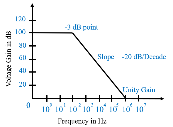
The frequency response of an OPAMP describes how its gain varies with frequency. While OPAMPs can ideally amplify signals across all frequencies, real-world devices have a limited bandwidth where gain starts to decrease at higher frequencies. Understanding the frequency response is essential when designing circuits for high-speed or high-frequency applications. Below diagram represents the frequency response of OPAMP:
Let’s break down the key elements:

Flat Region (Low Frequencies):
At lower frequencies, the op-amp maintains a constant voltage gain (around 100 dB in this case). This is the open-loop gain of the op-amp.
-3 dB Point:
This point marks the beginning of the roll-off. It is the frequency where the gain drops by 3 dB from the maximum value. This corresponds to the op-amp’s bandwidth limit for higher precision.
Roll-off Slope (-20 dB/decade):
Beyond the -3 dB point, the gain decreases at a rate of -20 dB/decade. This means the gain drops by 20 dB for every tenfold increase in frequency. This roll-off is typical of a single-pole system, which is common for op-amps.
Unity Gain Frequency:
The point where the gain reaches 0 dB (unity gain). It indicates the highest frequency at which the op-amp can amplify without any gain (effectively acting as a buffer).
Conclusion
Understanding these key characteristics of operational amplifiers is crucial for designing effective analog circuits. From gain control and input impedance to slew rate and frequency response, these parameters shape how OPAMPs function across various applications in signal processing, control systems, and instrumentation.

