Showing posts with label design flow. Show all posts

July 29, 2024

What is timing closure in VLSI design, and why is it important?

Timing closure in VLSI design refers to the process of ensuring that a digital circuit meets all its timing requirements, such as setup time, hold time, clock skew, and signal propagation delays, across all possible operating conditions and process variations. It is a critical step in the design flow that verifies the circuit can function correctly at the desired clock speed without timing violations.

Why Timing Closure is Important:

  • Ensuring correct circuit operation without timing violations is essential for functionality. Failure to achieve timing closure can lead to performance issues and errors.
  • Meeting timing requirements allows the circuit to run at its maximum clock speed, optimizing performance, especially in high-speed applications. Achieving timing closure guarantees reliability across varying conditions and is crucial for both consumer electronics and critical applications.
  • Proper timing closure also enhances power efficiency by minimizing unnecessary power consumption. Additionally, it facilitates manufacturing by reducing the risk of non-functional chips, improving yield, and lowering costs associated with re-spins and debugging.

Process of Timing Closure:

  • Achieving timing closure in VLSI design involves several critical steps. Static Timing Analysis (STA) is a key tool used for this purpose, analyzing the timing paths in the circuit without requiring dynamic simulation to ensure that all paths meet their timing requirements.
  • The process often involves iterative optimization, where adjustments are made to the design to fix timing violations. This can include resizing gates, adjusting placement and routing, and optimizing the clock tree.
  • Clock Tree Synthesis (CTS) is another crucial step, ensuring that the clock distribution network meets timing requirements, reducing skew and jitter.
  • Additionally, physical design adjustments, such as changes in placement, routing, and layout, are made to minimize delays and improve timing performance. Finally, sign-off verification is conducted to ensure that the design meets all timing constraints before tape-out.

In summary, timing closure is a vital aspect of VLSI design, ensuring that the circuit performs correctly and reliably at the desired speed, optimizing both performance and power efficiency.

March 28, 2023

A Journey Through CMOS Fabrication: A Comprehensive Guide with Diagrams.


Here, we will discuss CMOS fabrication of nMOS and pMOS structure on P-type substrate.

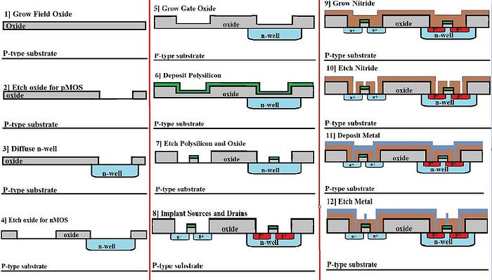
  • The below diagram shows how nMOS and pMOS can be fabricated on a P-type substrate.
  • From the above diagram, we can see that Source (S) and Drain(D) of pMOS has p+ type material and n-type channel. Similarly, Source (S) and Drain (D) of nMOS have n+ type material and p-type channel.
  • As we are fabricating nMOS and pMOS on P-type substrate we first need to have an n-well. For pMOS, we will first have an n-well and then have p+ material for Source and Drain. With p-type substrate, nMOS directly can be created with n+ Source and Drain.
  • Similarly, if we want to have nMOS and pMOS on N-type substrate then we will have a p-well of nMOS and pMOS will be directly created on N-type substrate.
  • Gate terminals are insulated for the channel material by the SiO2 layer.
    This oxide layer is thin at the gate and thick at the active(Source and Drain) region.
  • Steps for CMOS Fabrication are as follows:

Step 1: Create n well or p well region and channel stop region:
-For nMOS and pMOS special region must be created in which the semiconductor type will be opposite to the substrate type, these regions are called wells or tubes.
- p well is created on an n-type substrate and n well is created on a p-type substrate.
- nMOS transistors can be created on a p-type substrate or p well and pMOS transistors can be created on an n-type substrate or n well.
- That well should be of defined boundary to have fixed channel stop region to avoid crosstalk or mutual coupling effects.
- Refer Figures 1, 2, and 3.

Step 2: Grow field oxide or SiO2 (Thick Oxide) layer and gate oxide(Thin oxide).
- Thick oxide is grown on the active region of nMOS and pMOS.
- Thin gate oxide is grown on the surface through thermal oxidation.
- The oxidation process can be used to grow the SiO2 layer.
- Refer Figures 4 and 5.

Step 3: Deposit and Pattern Polysilicon layer:
- As per the circuit, make a pattern of the polysilicon layer.
- For implant Source and Drain terminals we now etch the polysilicon and SiO2 layer.
- Refer Figures 6 and 7.

Step 4: Implant source, the drain region, and substrate contacts:
- After having n well or p well regions, we create n+ or p+ regions for source, drain, and substrate.
- Refer Figures 8 and 9.

Step 5: Create contact windows, deposit, and pattern metal layer:
- Final metallization for metal interconnects.
- Refer Figures 10, 11, and 12.

In this way, we follow the above basic series of steps for CMOS Fabrication.

Like, Share, and Follow me if you like my content.
Thank You

The Journey of a Chip: Understanding the Complete Design Flow in VLSI.

Very Large Scale Integration (VLSI) is a process that integrates millions of transistors onto a single chip, revolutionizing the field of electronics. This intricate journey involves several critical steps, collectively known as the VLSI design flow. In this blog, we will explore each phase of this fascinating process, from initial specifications to the final testing and packaging.
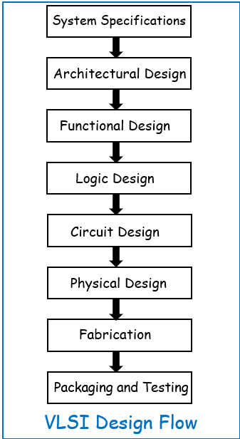
The below diagram shows the Design Flow in VLSI.

1. System Specifications

The journey begins with defining the system specifications. This phase sets the foundation for the entire design process by outlining performance targets, functionality requirements, physical dimensions, fabrication technology, and design techniques.

  • Performance: Speed, power consumption, and efficiency.
  • Functionality: Desired operations and features.
  • Physical Dimensions: Chip size constraints.
  • Fabrication Technology: Choice of technology node (e.g., 5nm, 7nm).
  • Design Techniques: Methodologies and tools to be used.

2. Architectural Design

Next, we move to architectural design, where the high-level structure of the chip is defined. This includes:

  • Module Definition: Defining modules in terms of inputs, outputs, and functionality.
  • ALUs and Floating Point Units: Determining the number and types.
  • Pipelines and Caches: Structure and sizes.

3. Functional Design

In functional design, we delve into detailed analysis and estimation of area, power, and performance parameters for each unit. This phase typically results in timing diagrams that illustrate how data moves through the system.

4. Logic Design

Logic design translates the functional design into a detailed logic representation.

  • Control Flow: Managing data and instruction flow.
  • Word Width and Register Allocation: Defining bit-widths and register usage.
  • Arithmetic and Logic Operations: Specifying operations and their implementations.

The outcome is an RTL (Register Transfer Level) description using HDLs like VHDL or Verilog.

5. Circuit Design

In this stage, the RTL description is converted into a circuit representation. Key considerations include:

  • Speed and Power Requirements: Ensuring the circuit meets performance goals.
  • Circuit Simulation: Verifying correctness and timing.

The result is a netlist, a detailed circuit diagram showing all components and their connections, often generated automatically using logic synthesis tools.

6. Physical Design

Physical design is perhaps the most complex phase, where the netlist is transformed into a geometric representation known as a layout.

  • Geometric Representation: Converting logic components into geometric shapes.
  • Layered Connections: Representing interconnections as lines across multiple layers.

7. Fabrication

Once the layout is verified, it’s time for fabrication. This involves:

  • Photolithographic Masks: Creating masks for each layer.
  • Wafer Processing: Growing silicon crystals, slicing wafers, and processing them according to the masks.

8. Packaging and Testing

The final step involves cutting the wafer into individual chips, packaging them, and conducting rigorous testing to ensure they meet all specifications.

Conclusion

The VLSI design flow is a complex and meticulously detailed process that transforms a concept into a functioning silicon chip. Each phase requires careful planning, precise execution, and thorough verification to ensure the final product performs as intended.

Explore Our Topics!

Check out the extensive list of topics we discuss:  Communication Protocols: -  USB   - RS232   -  Ethernet   -  AMBA Protocol: APB, AHB and...