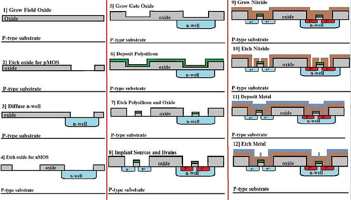
Here, we will discuss CMOS fabrication of nMOS and pMOS structure on P-type substrate.
- The below diagram shows how nMOS and pMOS can be fabricated on a P-type substrate.

- From the above diagram, we can see that Source (S) and Drain(D) of pMOS has p+ type material and n-type channel. Similarly, Source (S) and Drain (D) of nMOS have n+ type material and p-type channel.
- As we are fabricating nMOS and pMOS on P-type substrate we first need to have an n-well. For pMOS, we will first have an n-well and then have p+ material for Source and Drain. With p-type substrate, nMOS directly can be created with n+ Source and Drain.
- Similarly, if we want to have nMOS and pMOS on N-type substrate then we will have a p-well of nMOS and pMOS will be directly created on N-type substrate.
- Gate terminals are insulated for the channel material by the SiO2 layer.
This oxide layer is thin at the gate and thick at the active(Source and Drain) region. - Steps for CMOS Fabrication are as follows:
Step 1: Create n well or p well region and channel stop region:
-For nMOS and pMOS special region must be created in which the semiconductor type will be opposite to the substrate type, these regions are called wells or tubes.
- p well is created on an n-type substrate and n well is created on a p-type substrate.
- nMOS transistors can be created on a p-type substrate or p well and pMOS transistors can be created on an n-type substrate or n well.
- That well should be of defined boundary to have fixed channel stop region to avoid crosstalk or mutual coupling effects.
- Refer Figures 1, 2, and 3.
Step 2: Grow field oxide or SiO2 (Thick Oxide) layer and gate oxide(Thin oxide).
- Thick oxide is grown on the active region of nMOS and pMOS.
- Thin gate oxide is grown on the surface through thermal oxidation.
- The oxidation process can be used to grow the SiO2 layer.
- Refer Figures 4 and 5.
Step 3: Deposit and Pattern Polysilicon layer:
- As per the circuit, make a pattern of the polysilicon layer.
- For implant Source and Drain terminals we now etch the polysilicon and SiO2 layer.
- Refer Figures 6 and 7.
Step 4: Implant source, the drain region, and substrate contacts:
- After having n well or p well regions, we create n+ or p+ regions for source, drain, and substrate.
- Refer Figures 8 and 9.
Step 5: Create contact windows, deposit, and pattern metal layer:
- Final metallization for metal interconnects.
- Refer Figures 10, 11, and 12.

In this way, we follow the above basic series of steps for CMOS Fabrication.
No comments:
Post a Comment