- In the previous blog CMOS Fabrication Process, we have discussed the CMOS Fabrication Process of nMOS and pMOS on a p-type substrate.
- This fabrication process will have some disadvantages such as the crosstalk effect, latch-up effect, and mutual coupling.
- This will generate issues regarding the speed and performance of CMOS.
- To avoid those issues, we must fabricate nMOS and pMOS using Twin Tub Fabrication Process.
- The below diagram shows the final stage of the Twin Tub Fabrication Method.
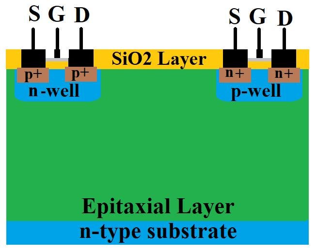
- Here, we will have two different wells n-well and p-well.
- nMOS will be fabricated on p-well and pMOS will be fabricated on n-well.
- Previously we have seen that nMOS and pMOS are fabricated on the p-type substrate but here we will have clear isolation between n-well and p-well which will help in avoiding issues regarding latch-up and mutual coupling.
- Steps for Twin Tub Fabrication Process are as follows:
Step 1] First we will have an n-type substrate with high resistance. Due to high resistance substrate current will be less. Higher resistivity can be obtained by having less doped n-type substrate.

Step 2] After that we will grow an Epitaxial Layer of n+ type material on the n-type substrate. This Epitaxial Layer will have a bit higher doping concentration than the n-type substrate. This layer will also have lesser resistance compared to the n-type substrate.

Step 3] Next we will grow a SiO2 layer above Epitaxial Layer and n-type substrate. The oxidation process can be used to grow the SiO2 layer.

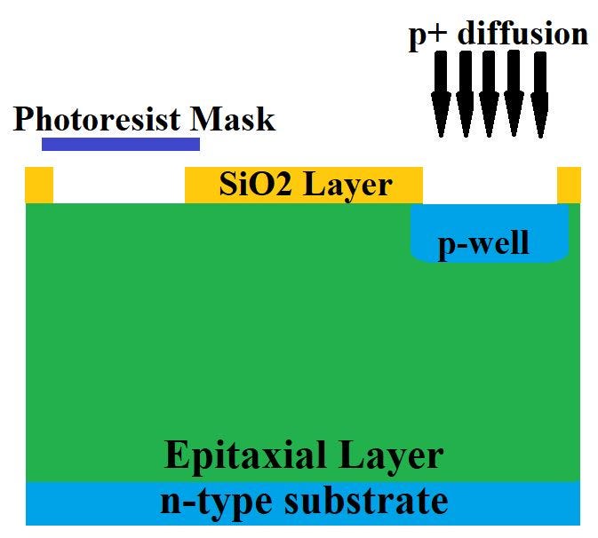
Step 4] Now we need to have n-well and p-well for nMOS and pMOS. Hence we will etch the SiO2 layer for n-well and p-well diffusion. SiO2 layer is etched using Masking. Two windows will be provided one for n well and the other for p well.

Step 5] After etching the SiO2 layer, we will be masking the 1st window by having photoresist material. and will have a diffusion of p+ material on the 2nd window to form p well.
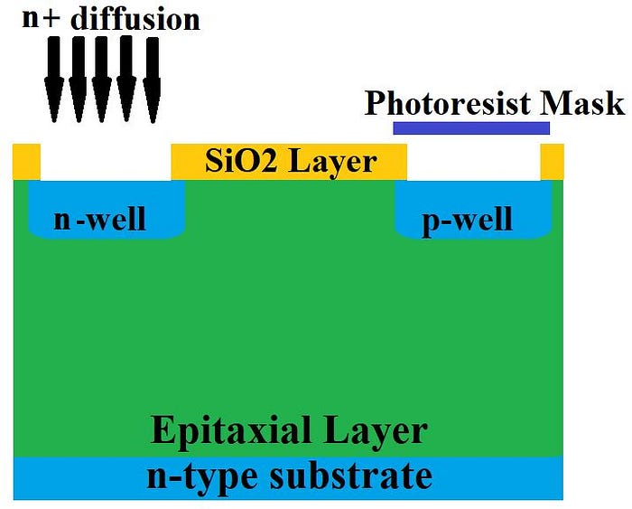
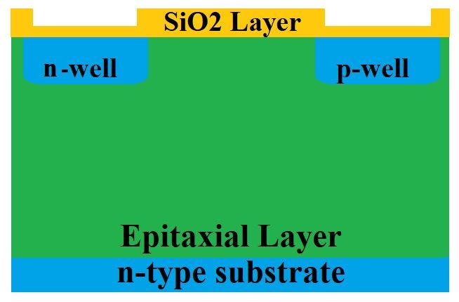
Step 6] Now we will mask the 2nd window by having photoresist material and diffuse the 1st window with n+ material to form n well.
Step 7] Now by having thermal oxidation we will be growing a thin SiO2 layer for having a Gate terminal.
Step 8] For photolithography and pattern making we will grow a polysilicon layer above the SiO2 layer.

Step 9] For implant Source and Drain terminals we now etch the polysilicon and SiO2 layer.
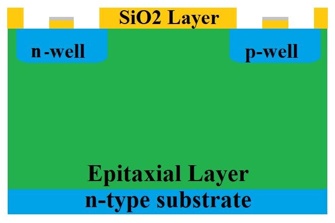
Step 10] After having the paths to grow source and drain terminals we will perform the masking steps again to form the two terminals. Here, first we will cover the 2nd window with photoresist material and diffuse the 1st window with p+ material to form Source and Drain.
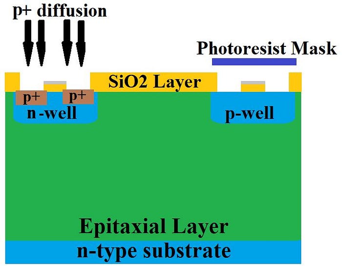
Step 11] After implanting Source and Drain terminals on n well, we now cover the 1st window and diffuse the 2nd window with n+ material for growing Source and Drain on the p well.

Step 12] After having the complete internal structure we now perform metallization for contact formation.
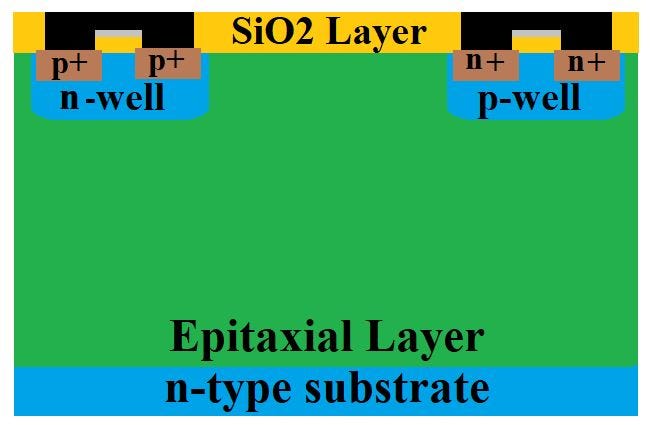
Step 13] After diffusion we need to cut this metal using metal etching to provide individual contacts for Gate, Source, and Drain.
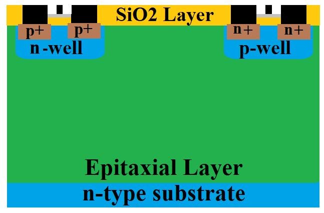
In this way, to avoid the issues with CMOS Fabrication Process, we use Twin Tub Fabrication Process.
No comments:
Post a Comment