Welcome to our exploration of VLSI (Very Large Scale Integration) design methodologies. In the realm of VLSI, designers have two primary approaches: Full Custom Design and Semi-Custom Design. Each has its strengths and weaknesses, catering to different project requirements and constraints.
1] Full Custom Design: Full Custom Design involves creating and verifying all components of a chip from the transistor level upward. This meticulous process allows for precise optimization of speed, power, and area, making it ideal for mass production. However, it comes with a trade-off — the design and production time of full custom designs are typically longer compared to semi-custom designs.
- Advantages of Full Custom Design:
- Optimized performance: Full custom designs can achieve higher performance levels compared to semi-custom designs.
- Area efficiency: By tailoring every component, full custom designs can minimize chip area.
- Power optimization: Fine-grained control over individual components enables power optimization.
- Disadvantages of Full Custom Design:
- Longer design and production time: Designing and verifying each component from scratch can be time-consuming.
- Not cost-efficient for small-scale projects: The high upfront investment in design and fabrication makes full custom design less suitable for low-volume productions.
2] Semi Custom Design: Semi-Custom Design offers a compromise between design flexibility and time-to-market constraints. In this methodology, pre-designed and pre-tested modules are used, with the option to customize and add additional components as needed. While it reduces design time, it may not be as optimized or cost-efficient for mass production compared to full custom design.
- Advantages of Semi-Custom Design:
- Reduced design time: Leveraging pre-designed modules accelerates the design process.
- Flexibility: Additional components can be integrated to meet specific requirements without starting from scratch.
- Suitable for low-volume productions: Semi-custom design offers a balance between customization and cost-effectiveness for smaller-scale projects.
- Disadvantages of Semi-Custom Design:
- Limited optimization: Pre-designed modules may not offer the same level of performance optimization as full custom designs.
- Higher production time: Despite faster design time, integrating and customizing modules can extend the overall production time.
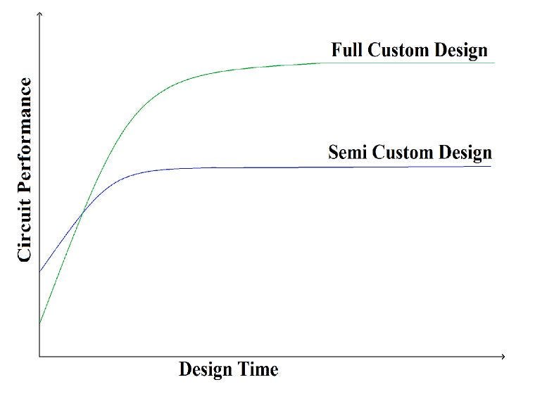
- Performance analysis of design methodology w.r.t design time:

From the above graph we can conclude following points:
- Initial circuit performance of the full custom design is less as compared to semi-custom design as we design it from the basic transistor level.
- Semi-custom has design less time compared to full custom design to get a stable circuit performance.
- Circuit performance of the full custom design is higher than the semi-custom design.
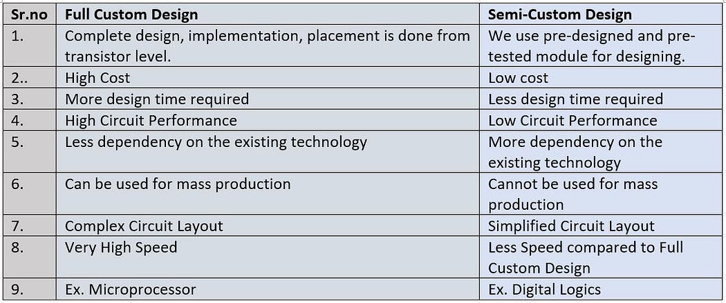
- Comparison between Full Custom and Semi-Custom design:

- Classification of Semi-Custom Design:
1] Standard Cell Design:

- The above diagram shows standard cells semi-custom design.
- Standard cells particularly use standard cell libraries which typically contain a few thousand cells, including inverters, Logic Gates, Adder circuits, Flip flops, AOI/OAI, etc.
- Each gate in this library will have its driving capabilities and parameters based on which we decide which block to be used.
- These standard cells have interconnects between them to perform different functions.
- The masking cost of standard cells is high.
- These cells can be used for both analog and digital designs.
- We don't perform floorplanning in a standard cell as blocks are already placed.
- Examples: Mux, Demux, Flip Flops, Logic Gates, Inverter, Adders, etc.
2] Gate Array Design:

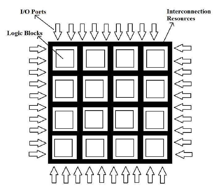
- The above diagram shows the structure of the Gate Array.
- Here, the position of logic blocks is fixed.
- These logic blocks can be connected using interconnection wires to perform different functions.
- Structure also has I/O ports for interfacing.
- Here we program wires and via to implement the desired functions.
- In the gate array, the logic blocks are already placed in pre-defined positions but not connected to each other.
- These gate arrays reduce making costs and also reduce design time.
- As the size, no of logic blocks, transistors are fixed efficiency is less.
3] Programmable Logic Devices:
- These are the IC that can be programmed according to the required specifications.
- Some PLDs are :
1] SPLD (Simple Programmable Logic Devices)
2] CPLD (Complex Programmable Logic Devices)
3] FPGA (Field Programmable Logic Devices) - Comparison between different Design styles:

In conclusion, both full custom and semi-custom design methodologies play crucial roles in VLSI design. While full custom design offers unparalleled optimization and performance, semi-custom design provides flexibility and faster time-to-market for smaller-scale projects. Understanding the strengths and weaknesses of each approach is essential for selecting the most suitable methodology based on project requirements and constraints.
No comments:
Post a Comment