Showing posts with label Digital Systems. Show all posts

September 6, 2024

Understanding the Full Subtractor: The Complete Subtraction Solution in Digital Electronics

In digital electronics, subtraction is as essential as addition, particularly when dealing with multi-bit numbers. While the Half Subtractor covers basic single-bit subtraction, it falls short when borrow operations come into play. The Full Subtractor is designed to handle these situations, making it a crucial element in advanced digital systems. This blog post will explore the Full Subtractor, its components, operation, and significance.

What is a Full Subtractor?

A Full Subtractor is a combinational circuit that performs the subtraction of two binary bits while accounting for a borrow from a previous stage. Unlike the Half Subtractor, which handles subtraction without borrow consideration, the Full Subtractor manages both the difference and borrow efficiently in multi-bit binary subtraction. It produces two outputs:

  • Difference (D)
  • Borrow (B_out)

Theoretical Background

Let’s revisit the rules of binary subtraction, adding the case where we borrow from a previous operation:

  • 0–0 = 0
  • 1–0 = 1
  • 1–1 = 0
  • 0–1 = 1 (with a borrow of 1)

When performing multi-bit subtraction, the Full Subtractor must also consider an input borrow (B_in) from the previous less significant bit, leading to more complex calculations.

Components of a Full Subtractor

A Full Subtractor involves three binary inputs:

  • A: The minuend (the number being subtracted from)
  • B: The subtrahend (the number being subtracted)
  • B_in: The borrow input from the previous stage

The Full Subtractor employs the following logic gates:

  • XOR Gates: To compute the difference
  • AND and OR Gates: To compute the borrow output

The logic expressions for the outputs are:

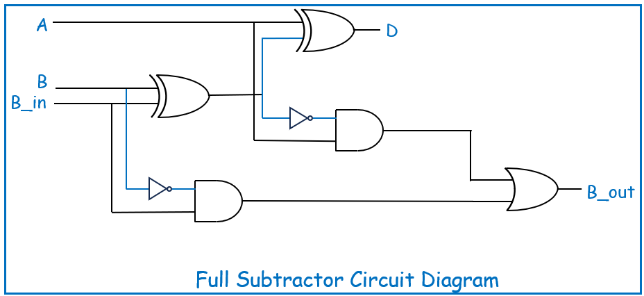
  • Difference (D) = A ⊕ B ⊕ B_in
  • Borrow out (B_out) = (A’ ANDB) OR ((A ⊕ B)’ AND B_in)

Circuit Diagram

The Full Subtractor circuit is built using the above components, showing how the XOR gates compute the difference and how the AND/OR gates handle the borrow. Here’s a simplified diagram for better understanding:
Truth Table

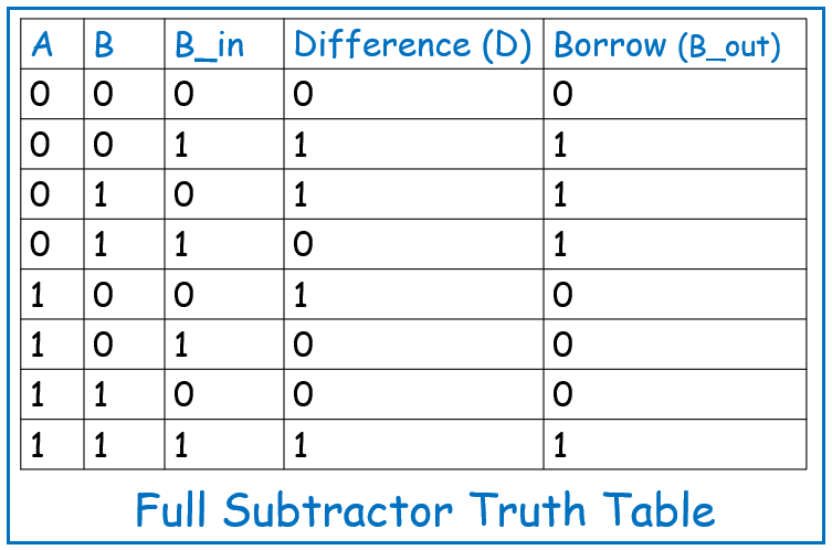
The Full Subtractor truth table details the results of all possible combinations of the three inputs (A, B, and B_in):
Applications of Full Subtractor

The Full Subtractor is vital in systems requiring multi-bit subtraction, including:

  • Arithmetic Logic Units (ALUs): A core component in CPUs for handling multi-bit arithmetic operations.
  • Digital Counters: Used in applications that require down-counting, where the Full Subtractor helps manage borrow operations.
  • Binary Calculators: Necessary for performing precise binary arithmetic.
  • Data Processing Systems: In systems requiring complex binary operations, the Full Subtractor plays a key role in ensuring accurate computations.

Conclusion

The Full Subtractor extends the functionality of the Half Subtractor by accounting for borrow operations, making it indispensable in multi-bit subtraction scenarios. Understanding the Full Subtractor’s logic and applications is essential for advancing in digital circuit design and gaining a deeper insight into how subtraction is handled in various digital systems. As you move toward more complex circuits, mastering the Full Subtractor will provide a strong foundation for future exploration in digital electronics.
September 4, 2024

Mastering Verilog: Part 9 — Diving into Tasks and Functions

In our ongoing journey to master Verilog, we’ve explored various foundational concepts and advanced features. In this segment, we will focus on two crucial constructs in Verilog programming: Tasks and Functions. Understanding these constructs is essential for creating modular, reusable, and efficient Verilog code.

1. Introduction to Tasks and Functions

Tasks and functions in Verilog are used to encapsulate and reuse code. They help in organizing code into manageable pieces, making it more readable and maintainable. While both tasks and functions serve similar purposes, they have distinct characteristics and use cases.

Often, we encounter repetitive code segments in RTL (Register Transfer Level) that are invoked multiple times. These segments typically do not consume simulation time and often involve complex calculations with varying data values. In such instances, declaring a function to encapsulate the repetitive code can be highly beneficial. A function allows you to process inputs and return a single value, reducing the amount of RTL code you need to write. By calling the function and passing the necessary data for computation, you streamline your code and avoid redundancy.

In contrast, a task is more versatile. Tasks can handle multiple result values, returning them through output or inout arguments. They can include simulation time-consuming elements like ‘@’ or ‘posedge’. While functions do not consume simulation time and return only a single value, tasks may or may not consume simulation time and can return values via output or inout arguments.

Verilog Tasks

A task in Verilog is used to perform a sequence of statements and can include delays and timing control. Tasks are useful for operations that may require multiple statements and potentially involve waiting periods.

Syntax:

task task_name;
// Input and output declarations
input [width-1:0] input_name;
output [width-1:0] output_name;

// Task body
begin
// Task operations
end
endtask

Example:

module TaskExample;
reg [7:0] a, b;
reg [7:0] result;

// Task Definition
task add_two_numbers;
input [7:0] num1, num2;
output [7:0] sum;
begin
#5 sum = num1 + num2; // Perform addition with a delay
end
endtask

initial begin
a = 8'd10;
b = 8'd20;
add_two_numbers(a, b, result); // Call the task
$display(“The result of addition is: %d”, result);
$stop;
end
endmodule

Explanation:
Task Definition: ‘add_two_numbers’ takes two inputs (‘num1’ and ‘num2’) and provides an output (‘sum’), with a delay of 5 time units before computing the sum.
Task Call: The task is invoked in the ‘initial’ block to perform the addition.

Key Features of Tasks:
- Can contain delays and timing controls.
- Can have input, output, and inout arguments.
- Can call other tasks.
- May or may not consume simulation time, depending on their contents.

Verilog Functions

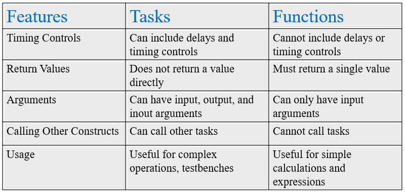
A function in Verilog is used for computing a value and returning it. Functions are typically used for simple calculations and must return a single value. They cannot contain delays or timing controls.

Syntax:

function [return_width-1:0] function_name;
input [input_width-1:0] input_name;
// Function body
begin
function_name = expression; // Compute and return value
end
endfunction

Example:

module FunctionExample;
reg [7:0] a, b;
reg [7:0] result;

// Function Definition
function [7:0] add_two_numbers;
input [7:0] num1, num2;
begin
add_two_numbers = num1 + num2; // Compute the sum
end
endfunction

initial begin
a = 8'd15;
b = 8'd25;
result = add_two_numbers(a, b); // Call the function
$display(“The result of addition is: %d”, result);
$stop;
end
endmodule

Explanation:
Function Definition: ‘add_two_numbers’ takes two inputs and returns their sum.
Function Call: The function is called in the ‘initial’ block to compute and return the result.

Key Features of Functions:
- Cannot contain delays or timing controls.
- Must return a single value.
- Cannot call tasks.
- Can be used within expressions.

Differences Between Tasks and Functions

Practical Examples

  1. Task Example
    Suppose you are designing a complex digital system where you need to perform a sequence of operations with delays. A task can be used to encapsulate this logic and improve code readability.
  2. Function Example
    For simple calculations such as computing a checksum or performing bitwise operations, functions can be used within expressions to streamline your code.

Conclusion

Tasks and functions are powerful constructs in Verilog that enable modular, reusable, and efficient coding practices. Tasks are suited for complex operations with timing controls, while functions are ideal for simple computations. By encapsulating repetitive code segments in functions and leveraging tasks for more complex operations, you can enhance code maintainability and efficiency. Mastering these constructs will elevate your ability to design and verify digital systems effectively.

Stay tuned for more insights and advanced topics in our mastering Verilog series!

July 1, 2024

Understanding the Half Subtractor: Essential Basics in Digital Electronics

In the realm of digital electronics, efficient subtraction operations are just as crucial as addition. The Half Subtractor, akin to its counterpart, the Half Adder, serves as a fundamental component in processing binary numbers. This blog post aims to elucidate the Half Subtractor, its operational principles, components, and significance in digital circuit design.

What is a Half Subtractor?

A Half Subtractor is a digital circuit designed to perform the subtraction of two single-bit binary numbers. Unlike the Full Subtractor, which handles borrow operations for multi-bit subtraction, the Half Subtractor operates without considering borrow. It produces two outputs: a difference bit (D) and a borrow bit (B).

Theoretical Background

Before delving into the Half Subtractor’s intricacies, let’s recap binary subtraction basics:

  • 0–0 = 0
  • 1–0 = 1
  • 1–1 = 0
  • 0–1 = 1 (with a borrow of 1)

Components of a Half Subtractor

A Half Subtractor comprises two essential logic gates:

  • XOR Gate: Computes the difference bit (D).
  • AND Gate: Computes the borrow bit (B).

The logical expressions governing these outputs are:

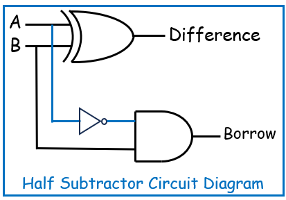
  • Difference (D) = A XOR B
  • Borrow (B) = A’ AND B

Here, A and B represent the binary inputs, and A’ denotes the complement of A.

Circuit Diagram

The circuit diagram for a Half Subtractor is straightforward, employing an XOR gate and an AND gate arranged as follows:

Truth Table

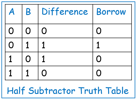
The truth table below illustrates the functionality of the Half Subtractor for all possible input combinations:

Applications of Half Subtractor

Half Subtractors find various applications in digital systems, including:

  • Building Full Subtractors: Essential for multi-bit subtraction operations, using Full Subtractors constructed from Half Subtractors.
  • ALUs (Arithmetic Logic Units): Integral to microprocessor design, where subtraction operations are crucial for arithmetic and logical calculations.
  • Binary calculators and digital counters: Used in devices requiring precise counting and data manipulation capabilities.
  • Error Detection: Utilized in checksum calculations for ensuring data integrity in communication and storage systems.

Conclusion

In summary, the Half Subtractor plays a pivotal role in digital electronics, facilitating the fundamental operation of binary subtraction. Its simplicity and essential function make it an indispensable component in the construction of more complex digital circuits. By grasping the operational principles and applications of the Half Subtractor, one gains a solid foundation in digital logic design, essential for advancing to more intricate digital systems and applications.

April 4, 2024

From Theory to Practice: CMOS Logic Circuit Design Rules Made Easy with Examples.

In the realm of VLSI circuit design, understanding CMOS (Complementary Metal-Oxide-Semiconductor) logic circuits is crucial. CMOS circuits are built using two types of transistors: nMOS (negative-channel Metal-Oxide-Semiconductor) and pMOS (positive-channel Metal-Oxide-Semiconductor). Let’s delve into the intricacies of CMOS logic design and explore how theory translates into practical circuitry.

  • Working Principles of nMOS and pMOS Transistors:
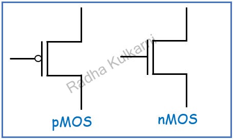
  1. nMOS: When the gate voltage is “0,” the nMOS transistor is OFF, acting as an open circuit. Conversely, with a gate voltage of “1,” it turns ON, behaving like a short circuit.
  2. pMOS: With a gate voltage of “0,” the pMOS transistor is ON, acting as a short circuit. When the gate voltage is “1,” it becomes OFF, akin to an open circuit.
  • Structure of CMOS Circuits:
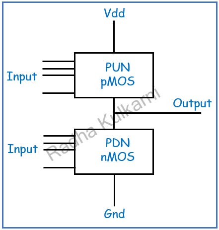
  1. CMOS circuits consist of a pull-up network made of pMOS transistors and a pull-down network made of nMOS transistors.
  2. The pull-up network connects to Vdd (the supply voltage) while the pull-down network connects to GND (ground).
  3. The output is derived from the connection between the pull-up and pull-down networks.
  4. pMOS transistors are efficient at passing logic high signals, while nMOS transistors excel at passing logic low signals.
  5. Due to the inherent inverting nature of CMOS, an inverter circuit is typically added at the output to obtain a non-inverted signal.
  • Basic Logic Circuit Rules:

In CMOS logic design, two fundamental operations are performed:

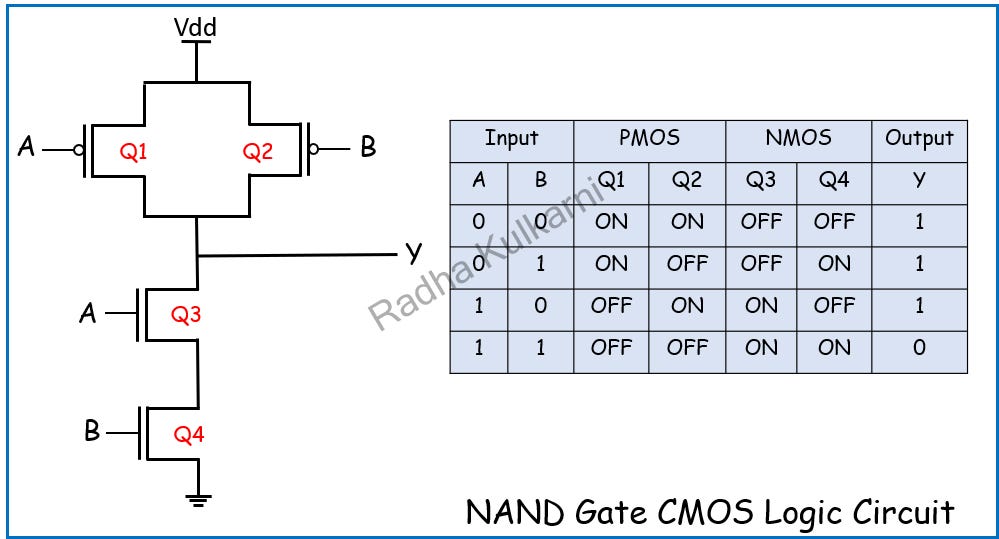
  1. The “ . “ operation, also known as the AND operation, involves connecting pMOS transistors in parallel and nMOS transistors in series.
  2. The “ + “ operation, or OR operation, connects nMOS transistors in parallel and pMOS transistors in series.
  • Examples:
  1. NAND Gate

2. NOR Gate

“Stay tuned for more examples and insights into CMOS logic design as we continue to explore the fascinating world of VLSI circuitry.”

In conclusion, understanding the intricacies of CMOS logic circuits, including the working principles of nMOS and pMOS transistors, the structure of CMOS circuits, and the basic logic circuit rules, is essential for anyone delving into VLSI circuit design. By grasping how theory translates into practical circuitry, we gain insights into creating efficient and robust digital systems.
Thank you for joining us on this exploration of CMOS logic design, and we look forward to sharing more knowledge and insights with you in the future.

Explore Our Topics!

Check out the extensive list of topics we discuss:  Communication Protocols: -  USB   - RS232   -  Ethernet   -  AMBA Protocol: APB, AHB and...