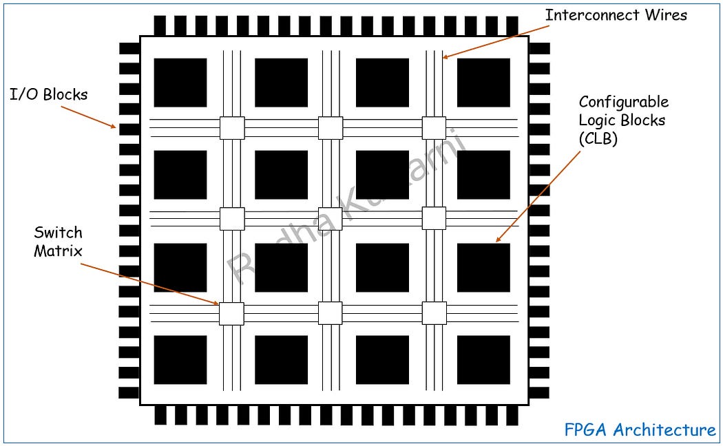
- FPGA, which stands for Field Programmable Gate Array, represents a programmable logic device allowing users to program or reprogram it post-manufacturing to meet specific requirements. Comprising a set of programmable logic blocks and interconnects, an FPGA can be tailored to execute a diverse range of digital operations.
- FPGAs are commonly programmed through Hardware Description Languages (HDLs) like VHDL (VHSIC Hardware Description Language) or Verilog, empowering designers to articulate the intended behavior of the digital circuits they aim to realize.
- FPGAs (Field-Programmable Gate Arrays) and ASICs (Application-Specific Integrated Circuits) are distinct types of integrated circuits with notable differences in design, functionality, and applications. FPGAs boast high flexibility and reprogrammability, contrasting ASICs, whose design remains fixed once manufactured.
- The predominant FPGA architecture encompasses a configuration of logic blocks known as configurable logic blocks (CLBs), along with I/O pads and routing channels.
- Typically, a logic block comprises a set of logical cells. Users can tailor CLBs to execute specific logic functions aligned with their design requirements. A standard cell encompasses a 4-input Look-Up Table (LUT), a full adder (FA), and a D-type flip-flop.
- The LUT may be partitioned into two 3-input LUTs, combined into a 4-input LUT through the initial multiplexer (mux) in normal mode. In arithmetic mode, their outputs are directed to the adder, with the mode selection programmed into the second mux. The output, whether synchronous or asynchronous, is contingent upon the programming of the third mux.
- FPGAs incorporate a grid of programmable interconnects, empowering users to establish connections among various CLBs. This flexibility facilitates the creation of data paths and control structures. The switch matrix stands as a pivotal component of the interconnect system, facilitating the routing of signals between CLBs.
- I/O Blocks serve as the crucial interface linking the FPGA to the external environment. Encompassing input buffers, output buffers, and bidirectional buffers, these blocks facilitate seamless communication with external devices.
- To define the FPGA’s functionality, users provide a design in a hardware description language (HDL) or through a schematic design. The HDL approach is particularly well-suited for handling large structures, allowing the specification of high-level functional behavior without the need to manually draw every component. On the other hand, schematic entry provides a more visual representation of the design and its modular components.
- Utilizing an electronic design automation (EDA) tool, a technology-mapped netlist is generated. This netlist is then adapted to the specific FPGA architecture through a process known as place and route, typically executed by the FPGA company’s proprietary place-and-route software. The user validates the results through timing analysis, simulation, and various verification and validation techniques. Upon the completion of the design and validation process, a binary file is generated, usually using the FPGA vendor’s proprietary software. This file is employed to (re-)configure the FPGA and is transferred to the device either via a serial interface (JTAG) or to an external memory device like an EEPROM.
- The most common HDLs are VHDL and Verilog as well as extensions such as SystemVerilog.
- Programming FPGA boards involves using a set of tools provided by FPGA vendors to design, synthesize, implement, and configure the FPGA with a specific digital circuit. Here are some commonly used tools in the FPGA programming process:
- Vivado (Xilinx)
- Quartus Prime (Intel FPGA)
- ModelSim (Mentor Graphics)
- VCS (Synopsys):
- Several companies specialize in the design and manufacturing of Field-Programmable Gate Arrays (FPGAs). Each vendor offers its own FPGA families, development tools, and support. here are some major FPGA vendors:
- Xilinx (AMD)
- Intel Corporation (Altera)
- Lattice Semiconductor
- Microchip Technology (Microsemi)
- Achronix Semiconductor
- QuickLogic Corporation
- Aldec, Inc.

