Check out the extensive list of topics we discuss:
- Tech and AI Blogs
- Communication Protocols:
- USB
- RS232
- Ethernet
- AMBA Protocol: APB, AHB and ASB
- UART, I2C AND SPI - Important concepts in VLSI:
- Designing a Chip? Here Are the 12 Important Concepts You Need to Know
- Metastability
- Setup time and Hold time
- Signal Integrity and Crosstalk effect
- Skews and Slack
- Antenna Effect - Semiconductor Memories
- Analog vs Digital Electronics
- Most Frequently Asked Questions in VLSI
- VLSI and Semiconductor Nuggets: Bite-Sized knowledge for Enthusiasts
- Common Acronyms in VLSI and Semiconductor Industry
- Transistors:
- BJT
- JFET
- MOSFET
- CMOS
- Transmission Gate CMOS
- Dynamic CMOS - Sequential Circuits:
- Registers
- Counters
- Latches
- Flip Flops - FPGA:
- ASIC vs FPGA
- FPGA Insights: From Concept to Configuration
- Full-Custom and Semi-Custom VLSI Designs: Pros, Cons and differences
- From Theory to Practice: CMOS Logic Circuit Design Rules Made Easy with Examples - CMOS Fabrication:
- CMOS Fabrication
- Twin-Tub CMOS Technology - Combinational Circuits
- Logic Gates
- Boolean Algebra and DeMorgan's Law
- Multiplexer (MUX) and Demultiplexer (DEMUX)
- Half Adder
- Full Adder
- Half Subtractor
- Full Subtractor
- Encoders
- Decoder - Analog Electronics
- OPAMP
- Inverting and Non-inverting Amplifiers
- Characteristics of OPAMP
- OPAMP Application: Adder, Subtractor, Differentiator, and More!
- Filters
- Hard Disk Drives Explained
- Passive Components: Capacitors and Resistors Explained
- LTSpice Tutorial 1: Installation and First Circuit Simulation - Verilog
- Verilog Datatypes
- Comments, Numeral Formats and Operators
- Modules and Ports
- assign, always and initial keywords
- Blocking and Non-Blocking Assignments
- Conditional Statements
- Looping Statements
- break and continue Statement
- Tasks and Functions
- Parameter and generate
- Verilog Codes - System Verilog:
- Disable fork and Wait fork.
- Fork and Join. - Project on Intel Quartus Prime and Modelsim:
- Vending Machine Controller - Xilinx Vivado Projects
1)VHDL
- Counters using Testbench code
- Flip Flops using Testbench code
- Logic Gates using Testbench code
- Full Adder using Half Adder and Testbench code
- Half Adder using Testbench code
2)Verilog
- Logic Gates using Testbench code
- Counters using Testbench code
- Full Adder using Half Adder and Testbench code
- Half Adder using Testbench code - VLSI Design Flow:
- Design Flow in VLSI
- Y chart or Gajski Kuhn Chart - Projects on esim:
- Step-by-Step guide on how to Design and Implement a Full Adder using CMOS and sky130nm PDK
- Step-by-Step guide on how to Design and Implement a Half Adder using CMOS and sky130nm PDK
- Step-by-Step guide on how to Design and Implement a 2:1 MUX using CMOS and sky130nm PDK
- Step-by-Step guide on how to Design and Implement a Mixed-Signal Circuit of 2:1 Multiplexer - IoT based project:
- Arduino
- Step-by-Step guide on how to Interface Load Cell using Arduino - Kmaps:
- Simplifying Boolean Equations with Karnaugh Maps - Part:2 Implicants, Prime Implicants and Essential Prime Implicants.
- Simplifying Boolean Equations with Karnaugh Maps - Part:1 Grouping Rules.
- Simplifying Boolean Equation with Karnaugh Maps.
- USB
- RS232
- Ethernet
- AMBA Protocol: APB, AHB and ASB
- UART, I2C AND SPI
- Designing a Chip? Here Are the 12 Important Concepts You Need to Know
- Metastability
- Setup time and Hold time
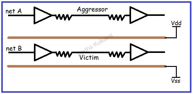
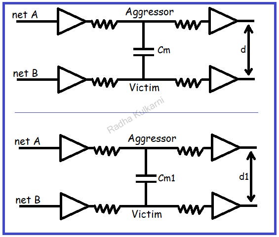
- Signal Integrity and Crosstalk effect
- Skews and Slack
- Antenna Effect
- BJT
- JFET
- MOSFET
- CMOS
- Transmission Gate CMOS
- Dynamic CMOS
- Registers
- Counters
- Latches
- Flip Flops
- ASIC vs FPGA
- FPGA Insights: From Concept to Configuration
- Full-Custom and Semi-Custom VLSI Designs: Pros, Cons and differences
- From Theory to Practice: CMOS Logic Circuit Design Rules Made Easy with Examples
- CMOS Fabrication
- Twin-Tub CMOS Technology
- Logic Gates
- Boolean Algebra and DeMorgan's Law
- Multiplexer (MUX) and Demultiplexer (DEMUX)
- Half Adder
- Full Adder
- Half Subtractor
- Full Subtractor
- Encoders
- Decoder
- OPAMP
- Inverting and Non-inverting Amplifiers
- Characteristics of OPAMP
- OPAMP Application: Adder, Subtractor, Differentiator, and More!
- Filters
- Hard Disk Drives Explained
- Passive Components: Capacitors and Resistors Explained
- LTSpice Tutorial 1: Installation and First Circuit Simulation
- Verilog Datatypes
- Comments, Numeral Formats and Operators
- Modules and Ports
- assign, always and initial keywords
- Blocking and Non-Blocking Assignments
- Conditional Statements
- Looping Statements
- break and continue Statement
- Tasks and Functions
- Parameter and generate
- Verilog Codes
- Disable fork and Wait fork.
- Fork and Join.
- Vending Machine Controller
1)VHDL
- Counters using Testbench code
- Flip Flops using Testbench code
- Logic Gates using Testbench code
- Full Adder using Half Adder and Testbench code
- Half Adder using Testbench code
2)Verilog
- Logic Gates using Testbench code
- Counters using Testbench code
- Full Adder using Half Adder and Testbench code
- Half Adder using Testbench code
- Design Flow in VLSI
- Y chart or Gajski Kuhn Chart
- Step-by-Step guide on how to Design and Implement a Full Adder using CMOS and sky130nm PDK
- Step-by-Step guide on how to Design and Implement a Half Adder using CMOS and sky130nm PDK
- Step-by-Step guide on how to Design and Implement a 2:1 MUX using CMOS and sky130nm PDK
- Step-by-Step guide on how to Design and Implement a Mixed-Signal Circuit of 2:1 Multiplexer
- Arduino
- Step-by-Step guide on how to Interface Load Cell using Arduino
- Simplifying Boolean Equations with Karnaugh Maps - Part:2 Implicants, Prime Implicants and Essential Prime Implicants.
- Simplifying Boolean Equations with Karnaugh Maps - Part:1 Grouping Rules.
- Simplifying Boolean Equation with Karnaugh Maps.

