- Very large scale integration (VLSI) is the process of creating an integrated circuit (IC) by combining thousands of transistors into a single chip. The design of a VLSI circuit follows a well-defined flow, starting from design specifications and ending at the fabrication and packaging of the chip.
- The VLSI design process consists of a series of steps that ensure the functionality and manufacturability of the chip.
- The below diagram shows the Design Flow in VLSI.
- To know more about the design flow, visit my blog The Journey of a Chip: Understanding the Complete Design Flow in VLSI.
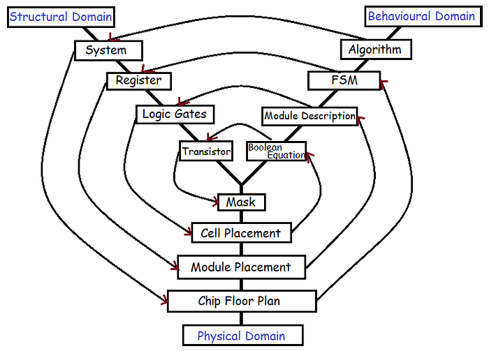
- To streamline this complex process, the Y-Chart or Gajski-Kuhn Chart is employed. This chart is a visual representation that simplifies the intricate relationships between the three key domains of VLSI design:
- Behavioural Domain: This is the starting point where the functionality of the chip is defined. It describes "what" the chip should do by specifying algorithms that define system behavior. In this stage, engineers focus on writing the high-level specifications that outline the intended operation of the IC.
- Structural Domain: Once the behavior is defined, the design moves into the structural domain. Here, the focus shifts to defining "how" the system will be built. The system is broken down into smaller modules and system components, such as logic gates, flip-flops, and registers. The structural domain is responsible for transforming the abstract behaviors into concrete components.
- Physical Domain: The final domain, the physical domain, deals with the physical realization of the chip. In this domain, the design is mapped onto silicon through processes like floorplanning, placement, and routing. Floorplanning algorithms determine where the various components should be placed on the chip, ensuring that the design adheres to timing constraints and power requirements.
- Y Chart or Gajski-Kuhn Chart is simply a pictorial representation of these three Domains in VLSI for better understanding the complete Design Flow.
- Below Diagram shows Y-Chart or Gajski-Kuhn Chart.
When we begin designing a VLSI circuit, the process starts with defining certain specifications. Based on these specifications, we formulate algorithms in the Behavioral Domain, which outline the intended functionality of the system. These algorithms are then passed on to the Structural Domain, where the system’s behavior is mapped onto specific hardware components. At this stage, system assignments are made, defining which logic gates, registers, and interconnects will execute the desired functions.
After defining the system’s structure, we move to the Physical Domain, where a chip floor plan is created using various floorplanning algorithms. The goal is to ensure an optimized physical layout that meets performance requirements such as power and area constraints.
Once the structure is physically mapped out, timing analysis is conducted to ensure that the design meets its timing constraints. This step, often involving tools like static timing analysis (STA), verifies the signal propagation times between components and registers defined in the Structural Domain. The system’s functionality over time, including clock cycles, is validated in this process.
Following this, module placement occurs in the Physical Domain, ensuring that components are aligned with the timing requirements determined during the timing analysis phase. The Behavioral Domain provides the high-level description of how the logic gates should operate, but the exact gate-level logic is synthesized in the Structural Domain and mapped during placement.
Considering the current-handling capabilities of different logic gates, we proceed to the cell placement stage, ensuring that logic blocks are positioned efficiently in the Physical Domain. The Boolean equations governing the behavior of the logic blocks are defined earlier in the synthesis phase (in the Structural Domain) and are then implemented using transistors, the fundamental building blocks of the design.
After verifying the circuit’s performance through simulation and validation, we move on to masking, the final stage. Here, physical connections are established between the logic blocks, enabling the design to function as a unified system, ready for fabrication.


No comments:
Post a Comment