- AMBA stands for Advanced Microcontroller Bus Architecture.
- What is a Microcontroller ??
A microcontroller is a small computer on a single VLSI integrated circuit (IC) chip. It comprises one or more CPUs (processor cores), as well as memory and programmable input/output peripherals. To facilitate communication between these internal components, a bus architecture is required. A Bus architecture includes system bus which is address bus + data bus +control bus. - Possible functional blocks on Board:
- One or more Microcontroller/ microprocessor.
- Memory — SRAM, DRAM, EPROM, Flash Memory.
- DSP — Digital Signal Processor.
- DMA — Direct Memory Access.
- USBs, SPI, I2C, IO ports, ADC/DAC, Timer.
- Definition of AMBA:
The ARM Advanced Microcontroller Bus Architecture (AMBA) is an open standard on-chip interconnect specification for connecting and managing functional blocks in a System-on-a-Chip (SoC). Developed by ARM, the AMBA specification has become the de facto standard for interfacing components within an SoC. - Essentially, the AMBA protocols define how functional blocks communicate with each other. They are used to minimize the silicon infrastructure, support modular system designs, and ensure system technology independence. AMBA protocols are widely used in a range of ASIC and SoC parts, including applications processors found in devices such as IoT devices, smartphones, and networking SoCs.
- AMBA Standards:
- AHB: Advanced High Performance Bus
- ASB: Advanced System Bus
- APB: Advanced Peripheral Bus
- ATB: Advanced Trace Bus
- AXI: AMBA Extensible Interface
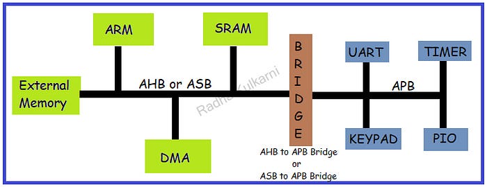
- The diagram below illustrates the AMBA (Advanced Microcontroller Bus Architecture) bus, consisting of the AHB (Advanced High-Performance Bus) and ASB (Advanced System Bus), as well as the APB (Advanced Peripheral Bus):
- In the diagram, the AHB/ASB is designed to handle high-performance and high-bandwidth modules or interfaces, including components such as memory, ARM (Advanced RISC Machines) processors, and DMA (Direct Memory Access) controllers.
- On the other hand, the APB is intended for low-bandwidth modules such as UART (Universal Asynchronous Receiver-Transmitter), Timer, Keypad, and PIO (Programmable Input/Output).
- To establish communication between these high and low bandwidth buses, a bridge is employed.
- The bridge serves as an intermediary, facilitating data transfer and control signals between the AHB/ASB and APB buses. This allows seamless integration of both high-performance and low-bandwidth modules within a larger system.
- APB:
- The Advanced Peripheral Bus (APB) is utilized for low-bandwidth peripherals.
- It facilitates the reading and writing of data between the bridge and the peripherals.
- In the architecture, the bridge functions as the master, while all the peripherals act as slaves.
- The APB employs the same signals for both read and write operations.
- It does not support burst transfers.
- Following are the different versions of AMBA APB with each having slight increased features than the previous:
- AMBA 2 APB : Basic read and write
- AMBA 3 APB : wait transfer and error response
- AMBA 4 APB : transaction protection and sparse data transfer.
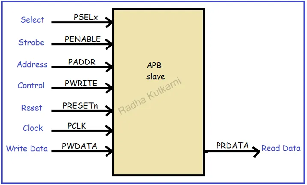
- The diagram below illustrates the signal description of the Advanced Peripheral Bus (APB) and its associated signals:
- PSELx: Slave selection signal, where ‘x’ represents the number of slaves.
The maximum width of signals in the APB is 32 bits. - PCLK: Clock signal.
- PRESETn: Reset signal.
- PADDR and PWRITE: Address and control signals used to determine whether a read or write operation should be performed on the bus. Typically, a value of 1 indicates a write operation, while 0 indicates a read operation. The address signal indicates the specific location or register to be accessed.
- PENABLE: Indicates when the access should occur.
- PWDATA and PRDATA: Data buses with a width of 32 bits, used for transferring data during read and write operations, respectively.
- Operation:
APB has three operating states: - idle
- Setup
- Access state
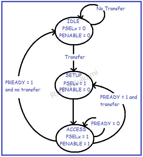
- IDLE: This is the default state of the APB. When a reset occurs, the bus enters the IDLE state. In this state, the enable signal is set to 0, and no slave is selected, resulting in no data transfer.
- SETUP: In the SETUP state, the slave to be selected for communication is determined. The corresponding PSELx signal is set to 1, while PENABLE remains at 0, indicating that the data transaction has not yet begun. When a transfer is required, the bus transitions to the SETUP state. During this phase, the bus waits for one clock cycle before moving to the ACCESS phase.
- ACCESS: In the ACCESS state, the PENABLE signal is set to high. The address, write_e, select, and write data signals must remain stable during the transition from the SETUP to ACCESS state. The ACCESS state is controlled by the PREADY signal. If PREADY is low (0), the bus remains in the same phase. If PREADY is high (1) and no data transfer is involved, the bus returns to the IDLE state. If a data transfer is required, the bus transitions back to the SETUP state for the next transaction. Based on the PWRITE control signal, data is either read from or written to the bus in this state. Any change in the PWRITE signal during this transition can result in data loss.
- Timing diagram:
- AHB and ASB:
- The Advanced High-Performance Bus (AHB) or Advanced System Bus is designed for interfaces requiring high bandwidth and high clock frequencies.
- It provides an efficient connection for processors, on-chip memories, and off-chip external memory interfaces.
- The AHB supports the concepts of multiple masters and multiple slaves, allowing for complex system configurations.
- Burst transfers are supported, enabling efficient data transfer in blocks.
- The AHB introduces several new features, including split transactions, single-cycle bus master handovers, single-clock-edge operation, and wider data bus configurations.
- The diagram below depicts the AHB protocol and its various components, including masters, slaves, address and control multiplexers, a read multiplexer, a write multiplexer, an arbiter, and a decoder.
- The two main characteristics of bus interface performances are:
- Bandwidth: It is the rate at which data can be driven across the interface. or can also be f=defined as number of bytes that can be transferred per second.
- Latency: This is the delay between start and end of the data transfer. or can be defined as how long does it take for data to go from memory to processor.
- Uses of AMBA:
- Efficient IP Reuse: AMBA facilitates the reuse of intellectual property (IP), allowing designers to leverage pre-existing modules and designs. This capability reduces development costs and shortens project timescales, as designers can incorporate proven components into their systems rather than developing everything from scratch.
- Compatibility and Flexibility: AMBA is a widely adopted standard, making it highly compatible with a variety of System-on-Chip (SoC) designs. It provides a flexible framework for connecting various components, allowing designers to seamlessly integrate different IP blocks from different vendors into a cohesive system.
- Scalability: AMBA supports different bus protocols, such as AMBA 5 AHB (Advanced High-Performance Bus) and AMBA 5 AXI (Advanced eXtensible Interface). This scalability enables designers to choose the appropriate bus protocol based on their specific requirements, ensuring optimal performance and resource utilization.
- Silicon Infrastructure Optimization: AMBA helps minimize silicon infrastructure requirements by providing efficient on-chip communication capabilities. It offers protocols and mechanisms for high-performance and low-power communication between IP modules, reducing the overall area and power consumption of the chip.
- Ecosystem Support: The popularity of AMBA has led to the development of a rich ecosystem of tools, IP blocks, and design methodologies. This ecosystem provides designers with a wide range of options and resources, enhancing productivity and enabling faster development cycles.
Now to interface all these functional blocks we need AMBA. AMBA is a System-on-Chip (SoC) bus architecture commonly used in microcontrollers.
The diagram below depicts the Finite State Machine (FSM) of the three states in the Advanced Peripheral Bus (APB):
The diagram below illustrates the timing diagram for an APB (Advanced Peripheral Bus) Write transfer with no wait state:
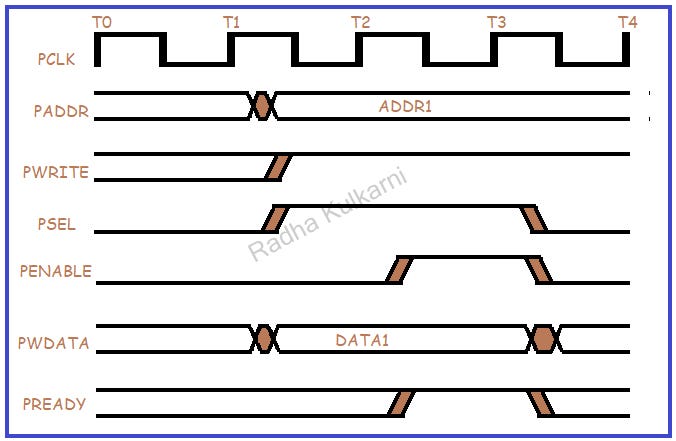
In the diagram:
The period from T0 to T1 represents the IDLE state, during which no data transaction occurs, and both the PSEL and PENABLE signals are low.
From T1 to T2, we enter the SETUP state where the address for the register is checked, and the decision to read or write data is made based on the PWRITE control signal. In this case, the PWRITE signal is set to 1, indicating a write operation, and we also check the PSEL signal. The SETUP state is entered only when PSEL is high. At this stage, PENABLE is still set to 0.
The period from T2 to T3 corresponds to the ACCESS state. Here, we set PENABLE to 1 and pay attention to the PREADY signal. The data from DATA1 will be stored or written in ADDR1 only when both the PENABLE and PREADY signals are 1.
Now, let’s consider the diagram for a Write transfer with a wait state:
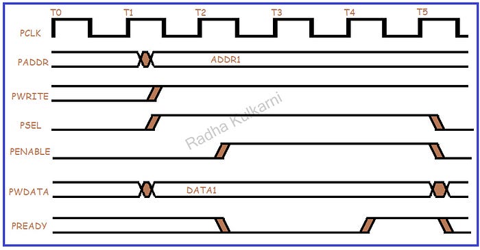
In this diagram, the transactions are similar to the previous one, with T0 to T1 representing the IDLE state, T1 to T2 as the SETUP state, and T2 to T3 as the ACCESS state. The difference lies in the ACCESS state, where data transitions only when the PREADY signal is 1. However, in this case, the PREADY signal is low (0), indicating that no data transition occurs between T2 and T3. Therefore, T3 to T4 becomes an extended ACCESS state where we wait for the PREADY signal to become high. This period, during which the ACCESS state is extended while waiting for the PREADY signal to transition the data from DATA1 to ADDR1, is referred to as a wait state transfer. Subsequently, between T4 and T5, the PREADY signal becomes 1, and the ACCESS state proceeds to transition the data, completing the operation within this period.
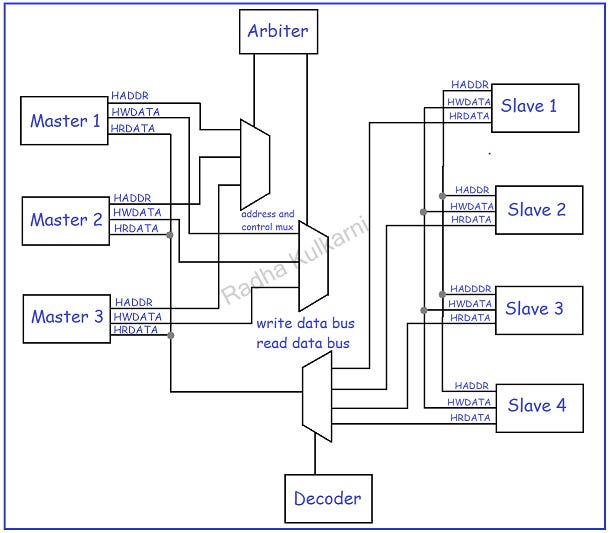
In the AHB (Advanced High-Performance Bus) architecture, there are 3 masters connected to 4 slaves. The HADDR bus is responsible for slave selection, allowing the masters to specify the target slave’s address. The HWDATA bus is used to transfer write data from the master to the selected slave, while the HRDATA bus is used for read data transfer from the slave back to the master.
To gain control of the bus and initiate a data transfer, a master sends a request to the arbiter. The arbiter grants access based on a prioritization scheme, ensuring that masters with higher priority are given access first. The decoder receives the address signal from the master and decodes it, generating slave select signals to identify the intended recipient. The slave responds to the master using the HRESP signal. Once the transfer is initiated, data is exchanged between the master and the slave. Additionally, there are other AHB signals employed, such as HCLK (the clock signal for the bus), HRESET (reset signal), HSELx (slave select signals for each slave), and HREADY (a signal indicating the readiness of the slave to accept data).
On the other hand, the ASB (Advanced System Bus) is a simplified version of the AHB, specifically designed for 16-bit and 32-bit systems. The ASB operates similarly to the AHB, starting with a master requesting access to the bus from the arbiter. Once the arbiter grants the request, the data transfer begins. The decoder decodes the address placed on the bus and selects the appropriate slave. The slave responds to the master, and the actual data transfer takes place. In the ASB, various signals are utilized, including BCLK (bus clock signal), BnRes (bus reset signal), BTRAN (transfer acknowledge signal), BWRITE (write signal), BERROR (error signal), and DSELx (slave select signals for each slave), among others.
A high performance and low performance bus cannot be connected directly. So, a compatible bridge such as AHB-APB or ASB-APB bus can be used.
The efficiency of your interface will depend on the extent to which it achieves the maximum bandwidth and zero latency.
Number of devices to be connected to the bus can also de one of the characteristics.
There are several significant benefits to using the AMBA (Advanced Microcontroller Bus Architecture) standard. These benefits include:
In summary, the AMBA standard offers benefits such as efficient IP reuse, compatibility and flexibility, scalability, optimization of silicon infrastructure, and a supportive ecosystem. These advantages contribute to reduced development costs, shorter timescales, and improved performance in SoC designs.