Showing posts with label Integrated Circuits. Show all posts

April 15, 2024

Explain the concept of Moore's Law and its impact on VLSI technology

Moore’s Law, named after Gordon Moore, a co-founder of Intel Corporation, refers to the observation made in 1965 that the number of transistors on a semiconductor chip roughly doubles every year. This prediction was later revised to every two years. This principle has had a profound impact on VLSI (Very Large Scale Integration) technology.

The essence of Moore’s Law lies in the exponential growth of transistor density on integrated circuits over time. This growth leads to increased computational power and functionality while reducing the cost per transistor. As a result, VLSI technology has experienced continuous advancement, enabling the creation of increasingly complex and powerful electronic devices.

The impact of Moore’s Law on VLSI technology can be summarized as follows:

  1. Enhanced Performance: Moore’s Law drives the development of smaller transistors, which in turn leads to higher clock speeds, improved processing power, and enhanced performance of VLSI chips. This advancement facilitates the design and implementation of more sophisticated electronic systems.
  2. Miniaturization: Transistor sizes shrink according to Moore’s Law, reducing the dimensions of VLSI chips and electronic devices. This miniaturization enables the production of smaller, lighter, and more energy-efficient devices like smartphones, tablets, wearables, and IoT devices.
  3. Cost Efficiency: The doubling of transistor density at regular intervals contributes to cost reductions in semiconductor manufacturing. This translates to lower production costs per transistor, making advanced VLSI technology more affordable and accessible.
  4. Innovation and Complexity: Moore’s Law fosters innovation and the development of complex VLSI designs. With more transistors available on a chip, designers can integrate intricate functionalities, advanced features, and specialized processing units, leading to groundbreaking advancements in computing, communication, and automation.
  5. Addressing Challenges: While Moore’s Law has historically driven progress, challenges such as physical limitations and technical hurdles have emerged in scaling transistor sizes further. This has prompted exploration of alternative technologies to sustain progress in VLSI technology.

In summary, Moore’s Law has been instrumental in driving the evolution of VLSI technology, resulting in faster, smaller, and more efficient electronic systems that have transformed various industries.

March 1, 2024

ASIC vs FPGA: Unveiling the Key Differences and Applications


  • In the realm of digital circuit design, two prominent technologies stand out: Application-Specific Integrated Circuits (ASICs) and Field-Programmable Gate Arrays (FPGAs). Each offers unique capabilities and is suited to different applications. This blog post delves into the comparative analysis of ASICs and FPGAs, shedding light on their advantages, disadvantages, and typical use cases.
  • The origins of ASICs and FPGAs trace back to distinct trajectories in the evolution of semiconductor technology. ASICs emerged as highly specialized integrated circuits tailored to specific applications, with their roots dating back to the early days of custom chip design.
  • Conversely, FPGAs arose as programmable logic devices, offering flexibility and reconfigurability to designers. Over time, both technologies have undergone significant advancements, catering to a broad spectrum of applications across industries.
  • Let’s break down the key differences between ASICs and FPGAs across various dimensions:

1] ASIC:

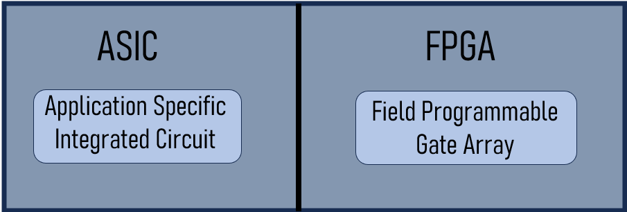
  • ASIC stands for Application-Specific Integrated Circuit. An ASIC is a type of integrated circuit (IC) customized for a specific application or use case. ASICs are created by designing and fabricating a semiconductor chip that integrates various electronic components and functionalities required for a specific application onto a single silicon die.
  • Unlike FPGAs, which are reconfigurable, ASICs are fabricated for a singular purpose, offering unparalleled performance and power efficiency. ASICs undergo a rigorous design process, including layout, fabrication, and testing, resulting in optimized solutions tailored to precise requirements.
  • ASICs can be further classified into two main categories:
  1. Full-Custom ASICs: In full-custom ASICs, every aspect of the design, including the layout of transistors and interconnects, is customized to meet the specific requirements of the application. Full-custom designs offer the highest level of performance and power efficiency but require significant time, expertise, and resources to develop.
  2. Semi-Custom ASICs: Semi-custom ASICs, also known as application-specific standard products (ASSPs), utilize pre-designed and pre-verified intellectual property (IP) blocks or modules, which are combined and configured to meet the application’s requirements. Semi-custom ASICs strike a balance between customization and time-to-market, offering faster development cycles and lower upfront costs compared to full-custom designs.
  1. Performance: ASICs excel in performance-critical applications, offering high-speed operation and low latency.
  2. Power Efficiency: With optimized designs and tailored architectures, ASICs minimize power consumption, making them ideal for battery-operated devices.
  3. Cost Efficiency: Despite higher initial development costs, ASICs can be more cost-effective in mass production scenarios due to lower per-unit costs.
  4. Security: ASICs provide enhanced security as their fixed designs make reverse engineering and tampering challenging.
  • Disadvantages of ASICs:
  1. NRE Costs: Non-Recurring Engineering (NRE) costs associated with ASIC development, including design, fabrication, and testing, can be substantial.
  2. Time to Market: ASIC development cycles are typically longer than FPGAs, resulting in extended time to market.
  3. Lack of Flexibility: Once fabricated, ASIC designs cannot be modified, limiting adaptability to changing requirements.
  4. Prototyping Challenges: Prototyping ASIC designs can be expensive and time-consuming, often requiring emulation or FPGA-based prototypes.
  • Typical Applications of ASICs:

ASICs are commonly used in a variety of industries, including telecommunications, automotive, aerospace, consumer electronics, and healthcare. They are deployed in diverse applications such as signal processing, data encryption, sensor interfaces, motor control, and networking equipment.

2] FPGA:

  • FPGA, which stands for Field Programmable Gate Array, represents a programmable logic device allowing users to program or reprogram it post-manufacturing to meet specific requirements. Comprising a set of programmable logic blocks and interconnects, an FPGA can be tailored to execute a diverse range of digital operations.
  • FPGAs are commonly programmed through Hardware Description Languages (HDLs) like VHDL (VHSIC Hardware Description Language) or Verilog, empowering designers to articulate the intended behavior of the digital circuits they aim to realize.
  • Click the link below for a comprehensive understanding of FPGAs:
    FPGA Insights: From Concept to Configuration
  • Advantages of FPGAs:
  1. Flexibility: FPGAs offer reconfigurability, allowing designers to implement and iterate designs quickly without the need for mask changes.
  2. Rapid Prototyping: FPGAs facilitate rapid prototyping, enabling designers to test and validate designs before committing to ASIC fabrication.
  3. Time to Market: FPGAs reduce time to market by enabling fast design iterations and prototyping, especially in dynamic market environments.
  4. Low NRE Costs: FPGAs eliminate the high upfront NRE costs associated with ASIC development, making them suitable for low-volume production and niche markets.
  • Disadvantages of FPGAs:
  1. Performance Limitations: FPGAs typically offer lower performance and higher power consumption compared to ASICs for equivalent tasks.
  2. Resource Constraints: FPGAs have finite resources (logic cells, memory, DSP blocks), which may limit the complexity and scale of designs.
  3. Cost per Unit: FPGAs can be more expensive per unit compared to ASICs for high-volume production runs.
  4. Security Concerns: FPGAs may be susceptible to security vulnerabilities such as bitstream manipulation and side-channel attacks.
  • Typical Applications of FPGAs:
  1. Prototyping and validation of ASIC designs in the early stages of development.
  2. Digital signal processing (DSP) applications including audio/video processing, communication systems, and image processing.
  3. Reconfigurable computing platforms for research, education, and experimentation.

In summary, both ASICs and FPGAs have their own strengths and are used for different jobs in digital circuit design. ASICs are like specialized experts — they’re really good at specific tasks, are energy efficient, and are hard to tamper with. On the other hand, FPGAs are more like versatile tools — they’re flexible, great for trying out new ideas quickly, and can be cheaper for smaller projects.

Deciding between ASICs and FPGAs depends on what you need for your project — like how fast it needs to be, how much money you have, and how quickly you need to finish. By understanding what each one is good at, engineers can choose the right tool for the job. Whether it’s making cars safer or building better computers, both ASICs and FPGAs help us create new and amazing things, shaping the future of technology.

Like, Share and Follow me if you like my content.
Thank You.

February 15, 2024

Non Volatile Memory


  • Non-volatile memory offers distinct advantages over volatile memory types like SRAM and DRAM. Unlike volatile memory, which loses data when power is removed, non-volatile memory retains stored data even in the absence of power. This feature ensures persistent storage, making it ideal for applications requiring long-term data retention.
  • One key advantage of non-volatile memory is that it doesn’t require periodic refreshing to maintain data integrity. This simplifies memory management and reduces overhead in system designs.
  • Non-volatile memory serves as secondary storage, providing consistent, long-term storage solutions. It complements volatile memory by offering larger storage capacities and persistence across power cycles.
  • This memory technology is extensively used in devices such as USB drives and digital cameras, where reliable data storage is essential. Moreover, with its higher speeds compared to traditional magnetic disks, non-volatile memory is rapidly replacing hard disk drives (HDDs) as secondary storage in computers, enhancing performance and efficiency.
  • ROM : Read-only memory (ROM) is an integrated circuit (IC) programmed with data during manufacturing and is widely used in electronic devices. ROM serves as a non-volatile storage solution where data cannot be deleted or overwritten by the user. Instead, all data is pre-programmed during the fabrication process using a ROM mask containing the necessary data.
  • While this lack of user modification may seem restrictive, it provides security by protecting data from tampering or unauthorized access.
  • ROM arrays can be implemented in two main ways: NOR-based ROM and NAND-based ROM.
  • Mask ROM is a specific type of ROM programmed by physically altering the IC during fabrication using a photolithographic mask. This process permanently sets the memory contents, typically representing firmware, software, or other data that needs to be stored permanently.
  • The data stored in mask ROM remains fixed once programmed, providing reliability and stability without the risk of data loss or corruption due to power outages or external factors.
  • However, this permanence comes with a limitation: the data cannot be modified or updated after programming. This lack of flexibility requires careful planning and verification during the design and manufacturing process to ensure the correct data is programmed into the memory.
  • PROM : Programmable Read-Only Memory (PROM) is a form of non-volatile memory that offers the unique ability to program data after the manufacturing process. Initially, PROM arrives blank, with all memory cells holding a default value. Unlike traditional ROM, PROM can be programmed by end-users post-manufacturing.
  • Programming typically involves applying electrical signals or voltage pulses to specific memory cells, altering their state from the default value to the desired configuration. Once programmed, the data becomes fixed and cannot be altered or erased. Similar to ROM, data stored in PROM remains intact even when power is removed, making it suitable for applications requiring long-term data storage.
  • Despite its flexibility, PROM does have limitations compared to other programmable memory technologies such as EEPROM or flash memory. Once programmed, the data in PROM remains unchanged, precluding any further modifications or erasures. This aspect makes PROM less suitable for applications requiring frequent updates or modifications.
  • EPROM : Erasable Programmable Read-Only Memory (EPROM) stores data that can be erased and reprogrammed as needed. The data erasure process involves exposing the EPROM cells to ultraviolet (UV) light through a transparent window on the chip.
  • The UV light makes the oxide layer conductive, generating electron-hole pairs in the material, effectively resetting the stored data. Depending on the intensity of the UV light source, the erasure process can take from a few seconds to several minutes, making it relatively slow.
  • Programming new data into EPROM is faster, typically taking 5–10 microseconds per word. However, one disadvantage of EPROM is the limited number of times it can be erased and reprogrammed, primarily due to the UV erase procedure.
  • Repeated erasures and reprogramming can also cause the threshold voltage of the EPROM cells to vary, leading to reliability issues. To mitigate this, EPROM chips often include an on-chip circuit to control the threshold voltage during programming.
  • During programming, EPROM consumes high power due to large channel currents and the requirement of high gate voltage, often around 12.5V. Despite this, EPROMs offer simplicity and higher density, enabling the manufacturing of large memory capacities at a relatively low cost.
  • EPROMs were commonly used in devices that did not require frequent programming. However, due to their limited reusability and reliability concerns, they have been largely replaced by Flash memory technology in modern applications.
  • EEPROM: EEPROM (Electrically Erasable Programmable Read-Only Memory) allows data to be erased by exposing the memory cells to an electric charge. Unlike traditional ROM, which is programmed once during manufacturing, EEPROM enables data to be stored or removed one byte at a time, offering flexibility in data management.
  • One of the key advantages of EEPROM is its ability to modify memory content without requiring additional devices or specialized equipment. Modern EEPROMs can perform multi-byte page operations, enabling efficient manipulation of larger blocks of data in a single operation.
  • Flash Memory: Flash memory is a non-volatile storage technology that retains data even when power is off. It operates by using floating-gate transistors to store electric charge, allowing data to be stored and retrieved over extended periods.
  • Data is written by applying charge to the floating gate (programming) and erased by removing the charge (resetting). Flash memory comes in two main types: NAND and NOR, with NAND commonly used in SSDs, USB drives, and memory cards, and NOR in devices requiring fast read access like microcontrollers and BIOS chips.

Explore Our Topics!

Check out the extensive list of topics we discuss:  Communication Protocols: -  USB   - RS232   -  Ethernet   -  AMBA Protocol: APB, AHB and...