Showing posts with label Semiconductor Technology. Show all posts

November 20, 2024

A Day in the Life of a Semiconductor: From Silicon to Superpower

Ever wondered what it’s like to be a semiconductor? Well, buckle up! Imagine waking up every morning in a lab with machines buzzing around you, ready to transform you into the brainpower behind everything from your smartphone to your self-driving car. Sounds exciting, right? Let’s take a quirky, fun-filled journey through a typical day in the life of a semiconductor, from dawn to dusk.
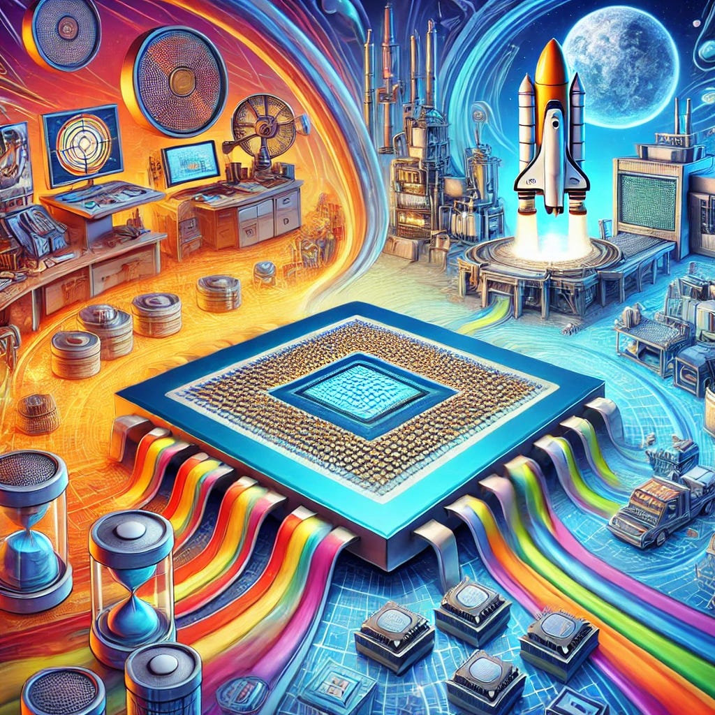
6:00 AM: Waking Up in the Lab

As the sun peeks through the high-tech windows, I’m already busy being prepared for my day. I’m a piece of silicon — just a tiny speck in the vast world of electronics. But don’t let my size fool you; I’m about to be turned into a microchip that powers some of the most complex and important technologies in the world.

I start my day on a giant wafer — yep, that’s my bed for now. Think of it as a shiny pancake that’s waiting to be transformed. But before I get into all the action, I have to endure hours of photolithography and etching. Fun fact: I don’t get a say in where I’m etched, but I’m cool with it. I’m designed to make a difference.

8:00 AM: The “Spa” Treatment

After the initial prep, it’s time for my first “spa treatment” — or, as the engineers like to call it, the cleaning process. I’m scrubbed, polished, and inspected to make sure I’m flawless. All those little imperfections — oh, they have no place here. I’ve got to be as smooth and perfect as a freshly baked cookie (minus the crumbs, of course).

I can feel the heat, the energy flowing through me as I get charged up. It’s not just a beauty treatment, it’s about getting me ready to be used in the most powerful machines on Earth. My pores — aka transistors — are etched to make sure I’m ready to carry out those complicated logic operations that humans love me for.

10:00 AM: Becoming a Transistor

Now comes the fun part — becoming transistors! You may have heard of them before. They’re the tiny switches that control the flow of electricity inside a chip. Every semiconductor like me has billions of them, and we work as a team to process data, compute, and keep everything running smoothly.

There’s a lot of excitement in the air. Each of us transistors is like a little worker in a massive factory, passing information back and forth. But don’t worry — there’s no chaos. It’s all organized. Just imagine a group of ants working together in perfect harmony, only we’re not ants. We’re much, much faster.

1:00 PM: Time to Meet the Chip Designers

After all that hard work, it’s time to meet the chip designers. This is the moment where all my carefully etched patterns and transistors are brought together into one beautiful, high-functioning microchip. It’s kind of like being in an assembly line, but with a lot more thoughtfulness. The designers make sure my architecture is perfect. My layout has to be just right: fast, efficient, and ready to take on the world.

There’s a lot of attention to detail — every little wire, every little connection needs to be in place for me to work flawlessly. Honestly, it’s a bit like playing Tetris, but with billions of tiny components instead of colorful blocks. The designers look happy, which means they’re pleased with how I’m shaping up. I’m almost ready for the big leagues!

3:00 PM: Enter the Testing Lab

After I’m assembled into my final form (a microchip, in case you were wondering), it’s time to go through some stress testing. This is where the fun begins! Think of it as an intense bootcamp for me.

The engineers run me through a battery of tests: electrical stress tests, thermal tests, and even mechanical tests. Will I survive the extreme conditions of space travel? Can I withstand the heat of a powerful computer? These tests will make sure I’m strong enough to handle anything. Honestly, I feel like I’m being prepped for my own action movie. The Semiconductor Chronicles: Rise of the Chips — anyone? 😜

5:00 PM: Packing Up for the Big Journey

After surviving the testing phase, I’m packed and shipped off to my new home. Whether I’m destined to be inside your smartphone, a supercomputer, or even a spaceship, this is the part of the day when I get to leave the lab and join the real world. It’s both exciting and nerve-wracking.

Will I become the powerhouse behind a groundbreaking technology? Or will I end up in a lesser-known device that simply sends emails and plays music? Either way, I’m ready. This is my destiny!

8:00 PM: A Well-Deserved Rest

At last, I’m installed into my final device. The user switches it on, and BOOM — I’m doing what I was born to do: powering everything behind the scenes. I might not get the credit for all the cool things my host device does, but I know that without me, none of it would work.

For now, it’s time for me to rest. Well, kind of. I’ll be on standby, waiting for the next task. After all, a semiconductor’s work is never truly done. From here, I’ll be activated and deactivated thousands of times, providing the power and processing abilities that make the world go round.

The Next Morning: Rinse and Repeat

And so, the cycle continues. Every day is a new adventure for a semiconductor like me. Sure, I may be small, but the impact I have on the world is anything but. From powering devices to enabling technology that can change the course of human history, I’m proud to be at the heart of it all.

So, the next time you power on your device, take a moment to appreciate the tiny chip inside. You may not see me, but I’m always there — doing my part to make the world a little smarter, faster, and more connected.

Liked this fun journey through the life of a semiconductor? Share it with your friends who love tech, and stay tuned for more quirky posts on electronics and technology!
March 1, 2024

ASIC vs FPGA: Unveiling the Key Differences and Applications


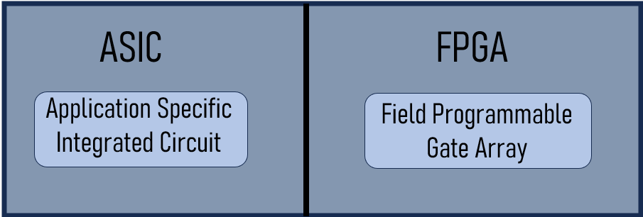
  • In the realm of digital circuit design, two prominent technologies stand out: Application-Specific Integrated Circuits (ASICs) and Field-Programmable Gate Arrays (FPGAs). Each offers unique capabilities and is suited to different applications. This blog post delves into the comparative analysis of ASICs and FPGAs, shedding light on their advantages, disadvantages, and typical use cases.
  • The origins of ASICs and FPGAs trace back to distinct trajectories in the evolution of semiconductor technology. ASICs emerged as highly specialized integrated circuits tailored to specific applications, with their roots dating back to the early days of custom chip design.
  • Conversely, FPGAs arose as programmable logic devices, offering flexibility and reconfigurability to designers. Over time, both technologies have undergone significant advancements, catering to a broad spectrum of applications across industries.
  • Let’s break down the key differences between ASICs and FPGAs across various dimensions:

1] ASIC:

  • ASIC stands for Application-Specific Integrated Circuit. An ASIC is a type of integrated circuit (IC) customized for a specific application or use case. ASICs are created by designing and fabricating a semiconductor chip that integrates various electronic components and functionalities required for a specific application onto a single silicon die.
  • Unlike FPGAs, which are reconfigurable, ASICs are fabricated for a singular purpose, offering unparalleled performance and power efficiency. ASICs undergo a rigorous design process, including layout, fabrication, and testing, resulting in optimized solutions tailored to precise requirements.
  • ASICs can be further classified into two main categories:
  1. Full-Custom ASICs: In full-custom ASICs, every aspect of the design, including the layout of transistors and interconnects, is customized to meet the specific requirements of the application. Full-custom designs offer the highest level of performance and power efficiency but require significant time, expertise, and resources to develop.
  2. Semi-Custom ASICs: Semi-custom ASICs, also known as application-specific standard products (ASSPs), utilize pre-designed and pre-verified intellectual property (IP) blocks or modules, which are combined and configured to meet the application’s requirements. Semi-custom ASICs strike a balance between customization and time-to-market, offering faster development cycles and lower upfront costs compared to full-custom designs.
  1. Performance: ASICs excel in performance-critical applications, offering high-speed operation and low latency.
  2. Power Efficiency: With optimized designs and tailored architectures, ASICs minimize power consumption, making them ideal for battery-operated devices.
  3. Cost Efficiency: Despite higher initial development costs, ASICs can be more cost-effective in mass production scenarios due to lower per-unit costs.
  4. Security: ASICs provide enhanced security as their fixed designs make reverse engineering and tampering challenging.
  • Disadvantages of ASICs:
  1. NRE Costs: Non-Recurring Engineering (NRE) costs associated with ASIC development, including design, fabrication, and testing, can be substantial.
  2. Time to Market: ASIC development cycles are typically longer than FPGAs, resulting in extended time to market.
  3. Lack of Flexibility: Once fabricated, ASIC designs cannot be modified, limiting adaptability to changing requirements.
  4. Prototyping Challenges: Prototyping ASIC designs can be expensive and time-consuming, often requiring emulation or FPGA-based prototypes.
  • Typical Applications of ASICs:

ASICs are commonly used in a variety of industries, including telecommunications, automotive, aerospace, consumer electronics, and healthcare. They are deployed in diverse applications such as signal processing, data encryption, sensor interfaces, motor control, and networking equipment.

2] FPGA:

  • FPGA, which stands for Field Programmable Gate Array, represents a programmable logic device allowing users to program or reprogram it post-manufacturing to meet specific requirements. Comprising a set of programmable logic blocks and interconnects, an FPGA can be tailored to execute a diverse range of digital operations.
  • FPGAs are commonly programmed through Hardware Description Languages (HDLs) like VHDL (VHSIC Hardware Description Language) or Verilog, empowering designers to articulate the intended behavior of the digital circuits they aim to realize.
  • Click the link below for a comprehensive understanding of FPGAs:
    FPGA Insights: From Concept to Configuration
  • Advantages of FPGAs:
  1. Flexibility: FPGAs offer reconfigurability, allowing designers to implement and iterate designs quickly without the need for mask changes.
  2. Rapid Prototyping: FPGAs facilitate rapid prototyping, enabling designers to test and validate designs before committing to ASIC fabrication.
  3. Time to Market: FPGAs reduce time to market by enabling fast design iterations and prototyping, especially in dynamic market environments.
  4. Low NRE Costs: FPGAs eliminate the high upfront NRE costs associated with ASIC development, making them suitable for low-volume production and niche markets.
  • Disadvantages of FPGAs:
  1. Performance Limitations: FPGAs typically offer lower performance and higher power consumption compared to ASICs for equivalent tasks.
  2. Resource Constraints: FPGAs have finite resources (logic cells, memory, DSP blocks), which may limit the complexity and scale of designs.
  3. Cost per Unit: FPGAs can be more expensive per unit compared to ASICs for high-volume production runs.
  4. Security Concerns: FPGAs may be susceptible to security vulnerabilities such as bitstream manipulation and side-channel attacks.
  • Typical Applications of FPGAs:
  1. Prototyping and validation of ASIC designs in the early stages of development.
  2. Digital signal processing (DSP) applications including audio/video processing, communication systems, and image processing.
  3. Reconfigurable computing platforms for research, education, and experimentation.

In summary, both ASICs and FPGAs have their own strengths and are used for different jobs in digital circuit design. ASICs are like specialized experts — they’re really good at specific tasks, are energy efficient, and are hard to tamper with. On the other hand, FPGAs are more like versatile tools — they’re flexible, great for trying out new ideas quickly, and can be cheaper for smaller projects.

Deciding between ASICs and FPGAs depends on what you need for your project — like how fast it needs to be, how much money you have, and how quickly you need to finish. By understanding what each one is good at, engineers can choose the right tool for the job. Whether it’s making cars safer or building better computers, both ASICs and FPGAs help us create new and amazing things, shaping the future of technology.

Like, Share and Follow me if you like my content.
Thank You.

Explore Our Topics!

Check out the extensive list of topics we discuss:  Communication Protocols: -  USB   - RS232   -  Ethernet   -  AMBA Protocol: APB, AHB and...