Pipelining is a technique used in digital circuits to increase throughput by dividing a process into multiple stages, each handled by different parts of the circuit simultaneously. By allowing multiple instructions to overlap in execution, pipelining improves the efficiency and speed of processing, as each stage completes part of the task in parallel with other stages. This technique is commonly used in CPUs and other high-speed digital systems to enhance performance.
Welcome to The Circuit Board – a knowledge hub dedicated to VLSI, semiconductors, and electronics. Our mission is to simplify complex concepts and share clear, engaging insights into the world of electronics engineering. From foundational principles to the latest industry trends, we cover a wide spectrum of topics to help learners, professionals, and enthusiasts stay informed.
July 28, 2024
December 12, 2023
Diving into Sequential Circuits: Part 4— Registers
- Flip flops are capable of storing 1-bit data, but to store more than 1 bit, registers are required. Registers, which are groups of flip flops, are employed to increase storage capacity. With n flip flops, it is possible to store an n-bit word using a single register.
- Binary data stored in registers can be shifted between flip flops using shift registers.
- A Shift Register is a group of flip flops used to store multiple bits of data and move the data from one flip flop to another. This shifting of data is accomplished using a clock signal. An n-bit shift register requires n flip flops. Shifting can occur either left or right using a Shift Left Register or Shift Right Register.
- Shift registers are classified into the following types:
- SISO (Serial In Serial Out)
- SIPO (Serial In Parallel Out)
- PISO (Parallel In Serial Out)
- PIPO (Parallel In Parallel Out)
- Bi-directional Shift Register
- Universal Shift Register
November 24, 2023
Mastering Verilog: Part 5 - Understanding Blocking and Non Blocking Statements
- Procedural Statements in Verilog, such as blocking and non-blocking assignments, are categorized as elements of procedural blocks, such as ‘always’ and ‘initial.’
- These statements play a crucial role in updating variables, and once a value is assigned, it remains unchanged until another procedural assignment modifies it. This stands in contrast to continuous assignments, where the value of a variable changes continuously.
- In procedural assignments, the order of signal assignments and the flow of execution are explicitly determined, providing control over the sequencing of operations within the design.
- Procedural blocks in Verilog primarily fall into two categories:
- always Blocks:
Usage: Utilized to describe both combinational and sequential logics, triggered by events such as a clock edge (posedge or negedge).
Example:
always @(posedge clk) begin
// Sequential or combinational logic here
end - initial Blocks:
Usage: Employed to specify initial conditions or setup during simulation, executing once at the beginning.
Example:
initial begin
// Initialization logic here
end
- Now let us see how these procedural statements work.
1] Blocking assignments:
- Syntax:
Specified using the ‘=’ operator. - Execution Flow:
Statements are executed sequentially in the order specified within the procedural block.
The execution of subsequent statements is blocked until the current assignment is completed. - Scope:
Blocking assignments within one procedural block do not impact the execution of statements in other procedural blocks. - Example:
Now let us consider below example to understand how blocking statements work. Below is not the complete verilog code but a module to understand the concept.
integer x,y,z;
initial
begin
x = 20;
y = 15;
z = 30;x = y + z;
y = x + 10;
z = x — y;
end
Now the output for above logic will be as follows:
initially, x=20,y=15,z=30
x becomes 45
y becomes 55
z becomes -10
- Initial Values:
Initially, the values of x, y, and z are set to 20, 15, and 30, respectively. - Execution Steps:
After the execution of the first statement (x = y + z), the value of x becomes 45.
The second statement (y = x + 10) utilizes the updated value of x (now 45), resulting in y becoming 55.
Finally, the third statement (z = x — y) uses the updated values of x (45) and y (55), causing z to become -10.
Provided below is the Verilog code for the logic mentioned above. Experiment with its implementation in simulation software to observe the output.
module blocking_assignment;
reg [31:0] x, y, z;initial begin
x = 20;
y = 15;
z = 30;// Blocking assignments
x = y + z; // x is assigned the value of y + z (15 + 30 = 45)
y = x + 10; // y is assigned the value of x + 10 (45 + 10 = 55)
z = x — y; // z is assigned the value of x — y (45–55 = -10)// Displaying the values after the assignments
$display(“x = %0d, y = %0d, z = %0d”, x, y, z);
end
endmodule
- Now let us consider the same example but with delays:
integer x,y,z;
initial
begin
x = 20;
y = 15;
z = 30;x = y + z;
#5 y = x + 10;
#10 z = x — y;
end
- Now the output for above logic will be as follows:
initially, x=20,y=15,z=30
x becomes 45
y becomes 55
z becomes -10
- Initial Values:
Initially, the values of x, y, and z are set to 20, 15, and 30, respectively. - Execution Steps:
After the execution of the first statement (x = y + z), the value of x becomes 45.
At time 0, the second statement (#5 y = x + 10) is scheduled to occur at time 5.
However, this scheduling doesn’t affect the immediate execution of the next statement.
At time 0, the third statement (#10 z = x — y) is scheduled to occur at time 10 + 5 = 15.
This means that the actual execution of the third statement occurs at time 15.
So, in the scenario with delays, the execution of the third statement (z = x — y) occurs at time 15, not immediately after the second statement. Therefore, the value of z becomes -10 at time 15.
2] Non Blocking Assignment:
- Syntax:
Specified using the ‘<=’ operator. - Key Characteristics:
Non-blocking assignments allow concurrent execution of statements within the same procedural block and do not block the execution of the next statement.
Particularly suitable for sequential logic implementation in Verilog, commonly used to model flip-flops and other sequential elements in digital circuits. - Sequential Logic Implementation:
Non-blocking assignments help avoid race conditions in sequential logic design.
When multiple signals are updated within the same clocked always block, non-blocking assignments ensure that all updates occur simultaneously at the next clock edge. - Example:
Let’s consider the same example used for blocking statements to illustrate how non-blocking statements work:
integer x, y, z;
initial begin
x = 20;
y = 15;
z = 30;x <= #10 y + z;
y <= #10 x + 10;
z <= #10 x — y;
end
- Output Explanation:
Initially, the values of x, y, and z are set to 20, 15, and 30.
After the execution of the statements at time 10 (due to delays), the values become:
x becomes 45
y becomes 30
z becomes -5 - Initially, the values of x, y, and z are set to 20, 15, and 30, respectively.
According to the given delay (#10), all statements within the initial block will execute at time 10 and will consider the initially defined values for calculation.
In conclusion, the significance of blocking and non-blocking assignments in Verilog coding cannot be overstated. These elements serve as the foundation for precise and effective digital circuit design, offering control over sequential and concurrent execution. As you venture further into the intricacies of Verilog, remember that mastering the art of assignments empowers you to create resilient and optimized digital systems. Happy coding!
Like, Share and Follow me if you like my content.
Thank You.
November 2, 2023
Verilog - NOT Gate
not_gate.v
module and_gate(a,y);
input a;
output y;
not(y,a);
endmodule
tb_not_gate.v
module tb_not_gate;
reg a;
wire y;
not_gate UUT (.a(a), .y(y));
initial begin
$display(“Testing NOT gate”);
a = 0;
#10;
$display(“Input_A = %b, Output = %b”, a,y);
a = 1;
#10;
$display(“Input_A = %b, Output = %b”, a,y);
$finish;
end
endmodule
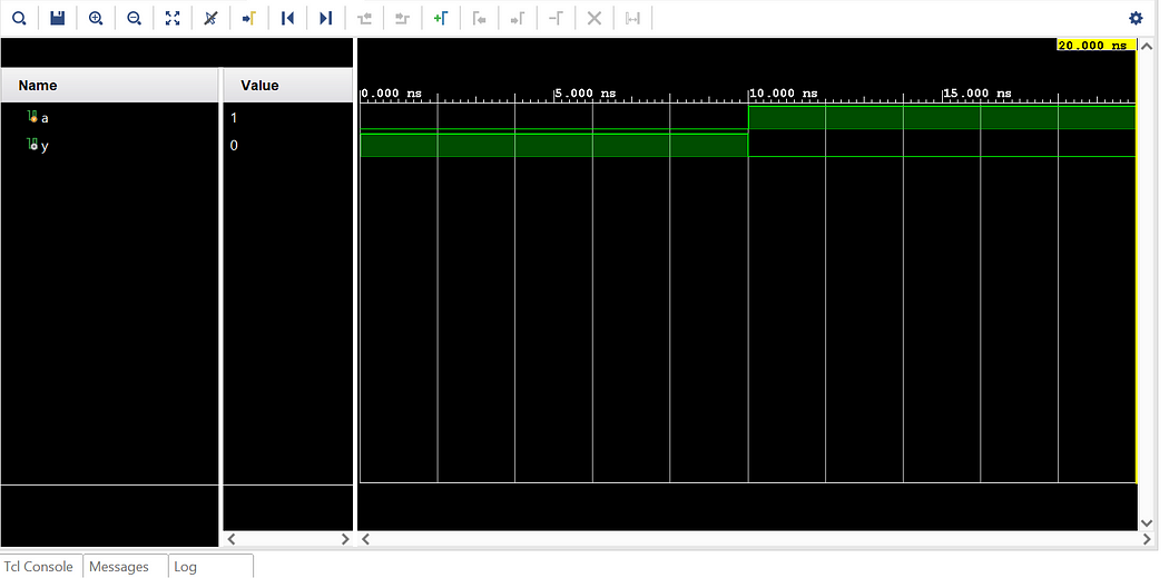
The output waveform for not gate will be as follows:
Verilog - XNOR Gate
xnor_gate.v
module xnor_gate(a,b,y);
input a;
input b;
output y;
xnor(y,a,b);
endmodule
tb_xnor_gate.v
module tb_xnor_gate;
reg a;
reg b;
wire y;
xnor_gate UUT (.a(a), .b(b), .y(y));
initial begin
$display(“Testing XNOR gate”);
a = 0; b=0;
#10;
$display(“Input_A = %b, Input_B = %b, Output = %b”, a,b,y);
a = 0; b=1;
#10;
$display(“Input_A = %b, Input_B = %b, Output = %b”, a,b,y);
a = 1; b=0;
#10;
$display(“Input_A = %b, Input_B = %b, Output = %b”, a,b,y);
a = 1; b=1;
#10;
$display(“Input_A = %b, Input_B = %b, Output = %b”, a,b,y);
$finish;
end
endmodule
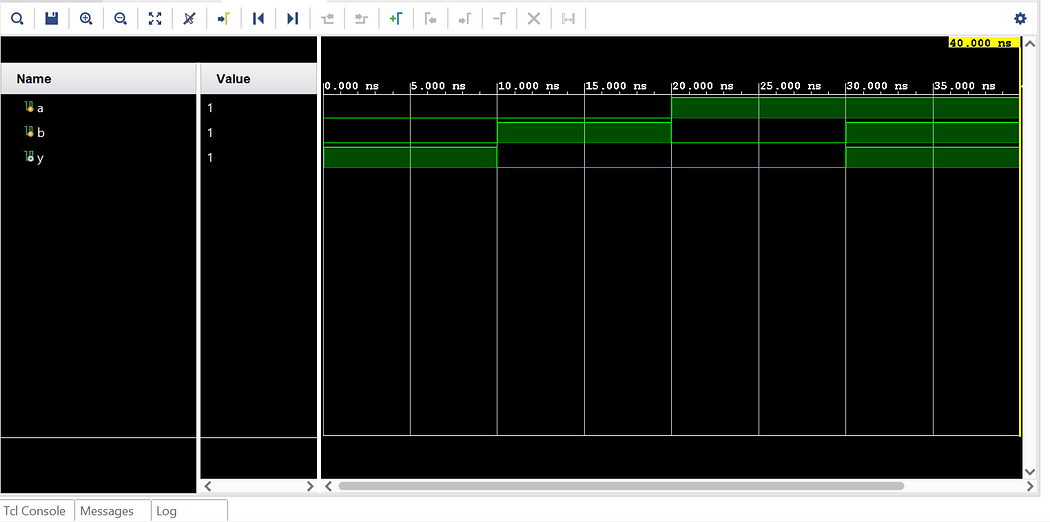
The output waveform for xnor gate will be as follows:
Verilog - XOR Gate
xor_gate.v
module xor_gate(a,b,y);
input a;
input b;
output y;
xor(y,a,b);
endmodule
tb_xor_gate.v
module tb_xor_gate;
reg a;
reg b;
wire y;
xor_gate UUT (.a(a), .b(b), .y(y));
initial begin
$display(“Testing XOR gate”);
a = 0; b=0;
#10;
$display(“Input_A = %b, Input_B = %b, Output = %b”, a,b,y);
a = 0; b=1;
#10;
$display(“Input_A = %b, Input_B = %b, Output = %b”, a,b,y);
a = 1; b=0;
#10;
$display(“Input_A = %b, Input_B = %b, Output = %b”, a,b,y);
a = 1; b=1;
#10;
$display(“Input_A = %b, Input_B = %b, Output = %b”, a,b,y);
$finish;
end
endmodule
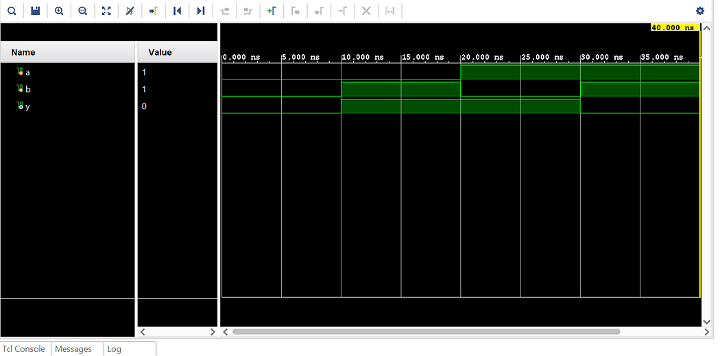
The output waveform for xor gate will be as follows:
Verilog - NOR Gate
nor_gate.v
module nor_gate(a,b,y);
input a;
input b;
output y;
nor(y,a,b);
endmodule
tb_nor_gate.v
module tb_nor_gate;
reg a;
reg b;
wire y;
nor_gate UUT (.a(a), .b(b), .y(y));
initial begin
$display(“Testing NOR gate”);
a = 0; b=0;
#10;
$display(“Input_A = %b, Input_B = %b, Output = %b”, a,b,y);
a = 0; b=1;
#10;
$display(“Input_A = %b, Input_B = %b, Output = %b”, a,b,y);
a = 1; b=0;
#10;
$display(“Input_A = %b, Input_B = %b, Output = %b”, a,b,y);
a = 1; b=1;
#10;
$display(“Input_A = %b, Input_B = %b, Output = %b”, a,b,y);
$finish;
end
endmodule
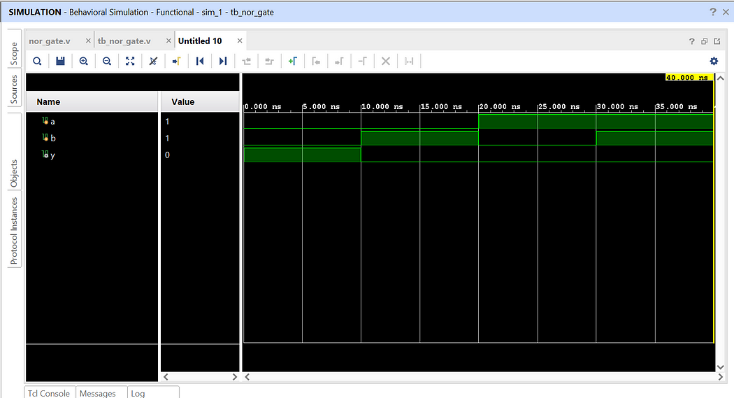
The output waveform for nor gate will be as follows:
Verilog - NAND Gate
nand_gate.v
module nand_gate(a,b,y);
input a;
input b;
output y;
nand(y,a,b);
endmodule
tb_nand_gate.v
module tb_nand_gate;
reg a;
reg b;
wire y;
nand_gate UUT (.a(a), .b(b), .y(y));
initial begin
$display("Testing NAND gate");
a = 0; b=0;
#10;
$display("Input_A = %b, Input_B = %b, Output = %b", a,b,y);
a = 0; b=1;
#10;
$display("Input_A = %b, Input_B = %b, Output = %b", a,b,y);
a = 1; b=0;
#10;
$display("Input_A = %b, Input_B = %b, Output = %b", a,b,y);
a = 1; b=1;
#10;
$display("Input_A = %b, Input_B = %b, Output = %b", a,b,y);
$finish;
end
endmodule
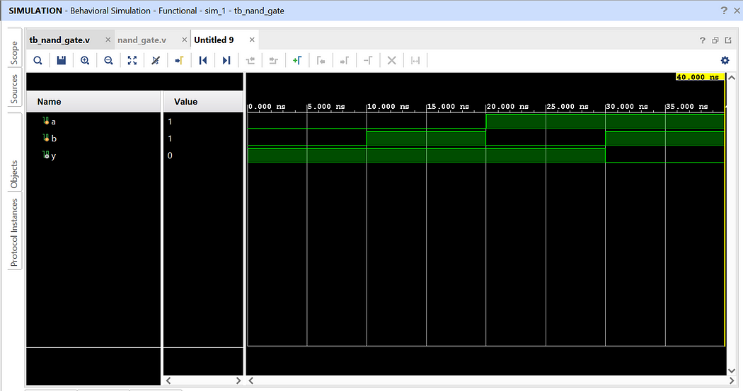
The output waveform for nand gate will be as follows:
Verilog - Or Gate
or_gate.v
module or_gate(a,b,y);
input a;
input b;
output y;
or(y,a,b);
endmodule
tb_or_gate.v
module tb_or_gate;
reg a;
reg b;
wire y;
or_gate UUT (.a(a), .b(b), .y(y));
initial begin
$display(“Testing OR gate”);
a = 0; b=0;
#10;
$display(“Input_A = %b, Input_B = %b, Output = %b”, a,b,y);
a = 0; b=1;
#10;
$display(“Input_A = %b, Input_B = %b, Output = %b”, a,b,y);
a = 1; b=0;
#10;
$display(“Input_A = %b, Input_B = %b, Output = %b”, a,b,y);
a = 1; b=1;
#10;
$display(“Input_A = %b, Input_B = %b, Output = %b”, a,b,y);
$finish;
end
endmodule
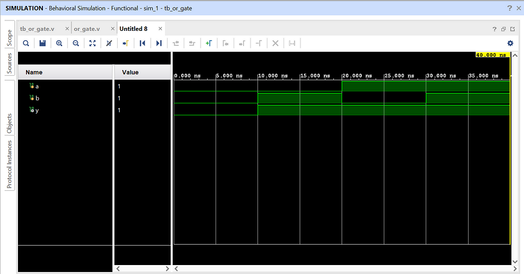
The output waveform for or gate will be as follows:
November 1, 2023
Step-by-step guide on how to design and implement a Half Adder using Testbench code with Xilinx Vivado design tool using Verilog HDL.
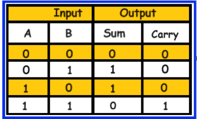
Half Adder is a combinational logic circuit that adds two inputs and produces two outputs. The diagram below illustrates the basic block diagram and circuit diagram of a Half Adder, where A and B are the inputs, and Sum and Carry are the outputs.

The table below presents the truth table of a Half Adder.
The output equations of a Half Adder is as follows:

In this project, we will design and implement the Half Adder using Testbench code with the Xilinx Vivado design tool using Verilog HDL.
Step 1: Click on New Project -> Next

Step 2: Enter Project Name and Select appropriate Project Location -> Next

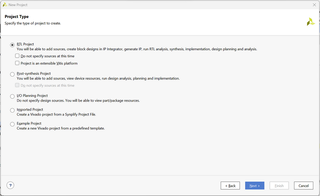
Step 3: Select RTL Project -> Next
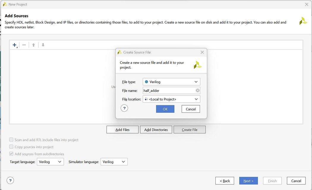
Step 4: Click on Create File and create 3 files with file name half_adder-> Next
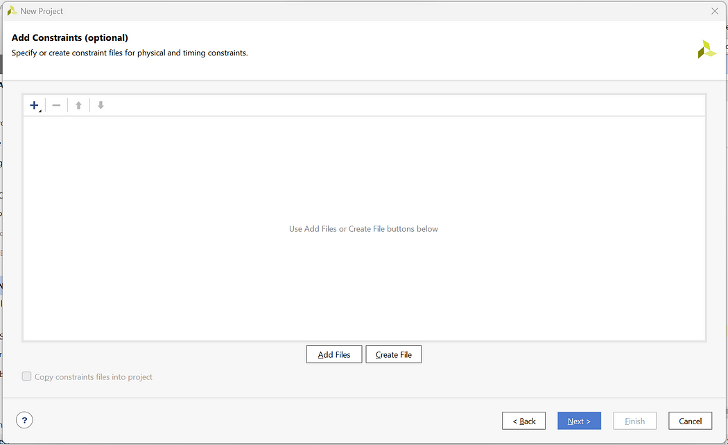
Step 5: We will not add the Constraint file So click on Next
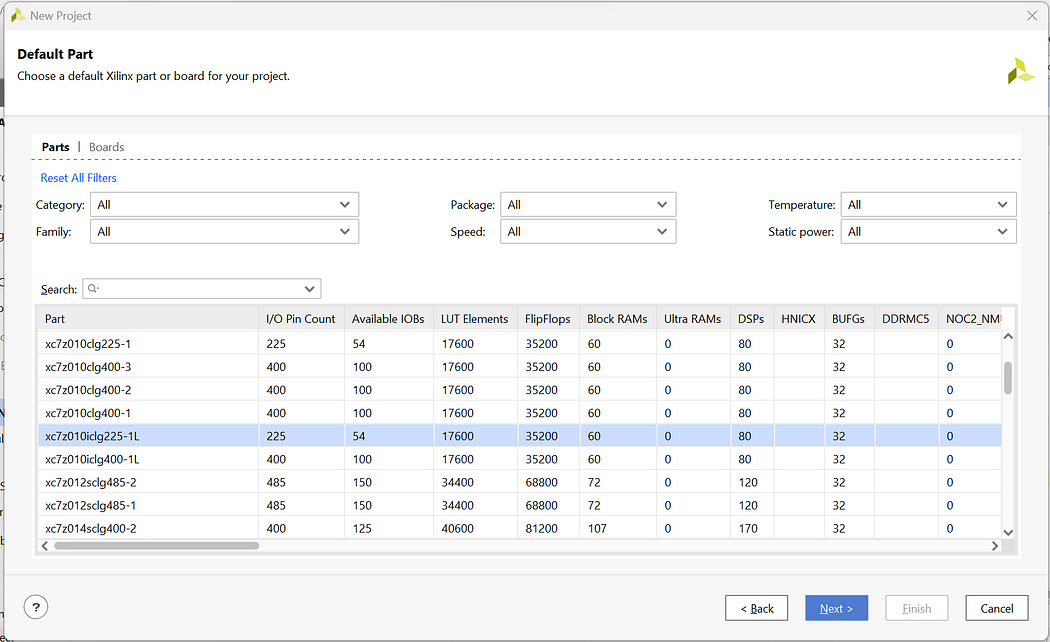
Step 6: For Default Part click on Next as we are not using any development Board
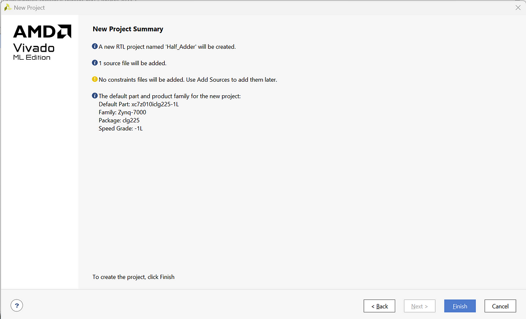
Step 7: Check the New Project Summary and click on Finish
Step 8: Now you will be prompted with the Define module page but we will create the complete code from scratch so click on cancel and Yes
Step 9: Now on the Home Page click on Sources -> Design Sources -> Non-module Files
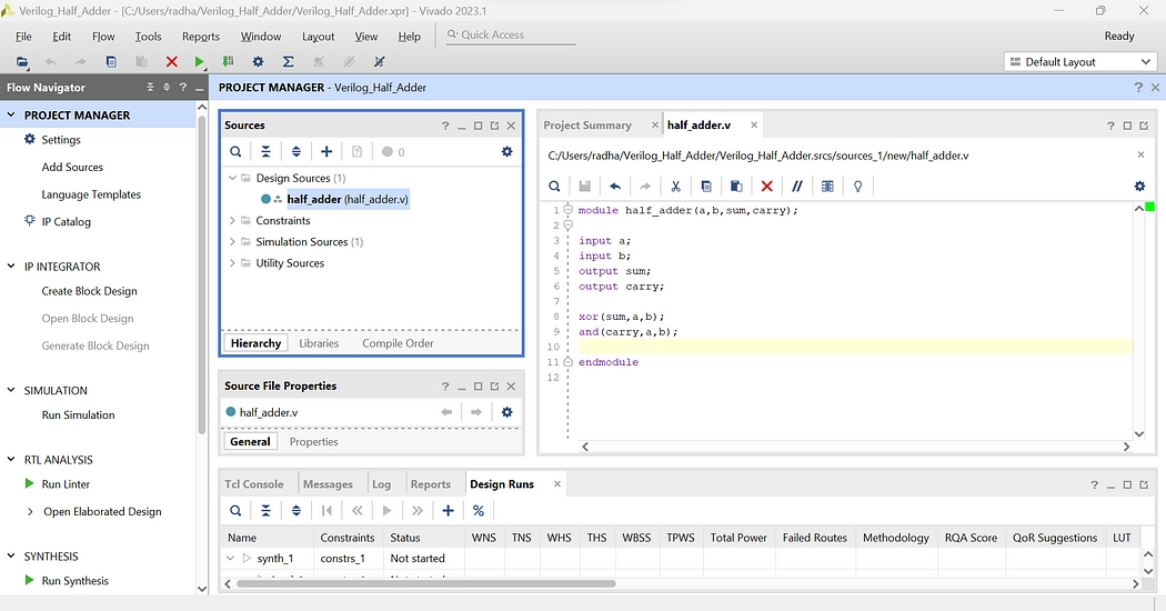
Step 10: Enter the below codes in the “half_adder.v” files.
module half_adder(a,b,sum,carry);
input a;
input b;
output sum;
output carry;
xor(sum,a,b);
and(carry,a,b);
endmodule
Step 11: Now to write the testbench code for above design right click on Design Sources -> Add Sources -> Add or create design sources -> Create File -> Add File name as tb_half_adder -> Finish -> Ok -> Yes
Step 12: Now open the testbench file and enter the below testbench code
module tb_half_adder;
reg a;
reg b;
wire sum;
wire carry;
half_adder UUT (.a(a), .b(b), .sum(sum), .carry(carry));
initial begin
$display(“Testing Half Adder gate”);
a = 0; b=0;
#10;
$display(“Input_A = %b, Input_B = %b, Sum = %b, Carry = %b” , a,b,sum,carry);
a = 0; b=1;
#10;
$display(“Input_A = %b, Input_B = %b, Sum = %b, Carry = %b” , a,b,sum,carry);
a = 1; b=0;
#10;
$display(“Input_A = %b, Input_B = %b, Sum = %b, Carry = %b” , a,b,sum,carry);
a = 1; b=1;
#10;
$display(“Input_A = %b, Input_B = %b, Sum = %b, Carry = %b” , a,b,sum,carry);
$finish;
end
endmodule
Here, in testbench code we do not define values in entity hence we have kept it empty. Then in architecture we have copied the components of half_adder and defined signals for connecting the ports of half adder. Inside the process statement we write all 4 test cases from truth table and define the respective delays.
Step 13: Now as we have written all the codes let’s launch the simulation. Enter launch_simulation in the Tcl Console and press Enter.
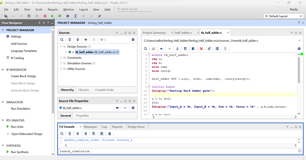
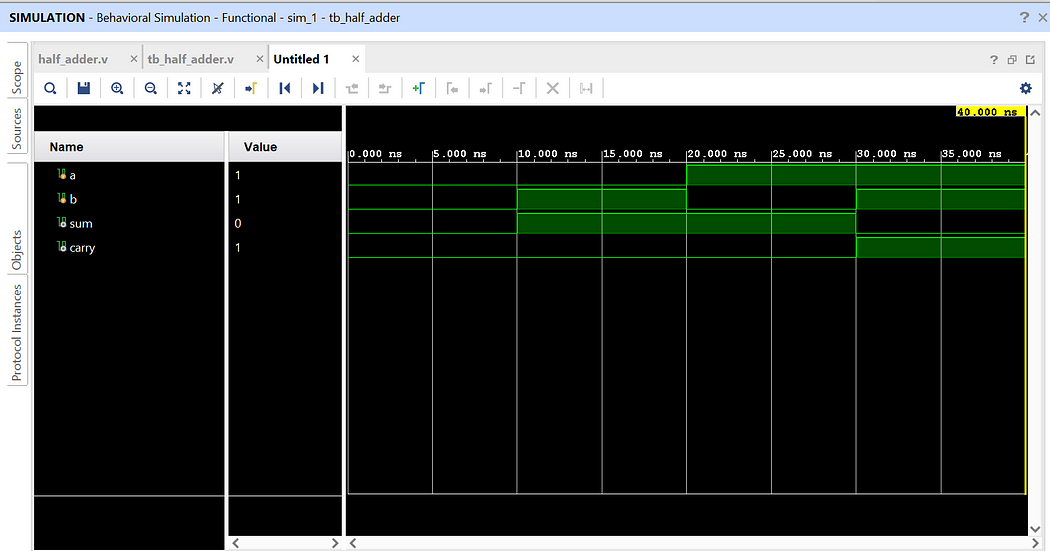
We have successfully implemented half adder with testbench code. Click on Zoom Fit to see the output waveform more clearly and verify the outputs.
Like, Share, and Follow me if you like my content.
Thank You
Explore Our Topics!
Check out the extensive list of topics we discuss: Tech and AI Blogs Communication Protocols: - USB - RS232 - Ethernet - AMBA Prot...
-
AMBA stands for Advanced Microcontroller Bus Architecture. What is a Microcontroller ?? A microcontroller is a small computer on a single ...
-
An amplifier is an electronic device or circuit that increases the power, voltage, or current of an input signal. Amplifiers are a crucia...
-
In System Verilog, a thread or process is a segment of code that operates independently as a distinct entity. During the verification proces...