In my previous blog I have explained what latches are. Now, let us consider flip flops:
Flip-flops or latches are circuits that function as bistable multivibrators, capable of storing one bit of binary data. Once set to a particular state, they will remain in that state until directed by an input to change their state.
1] SR flip flop:
The below diagram shows circuit diagram for SR flip flop:
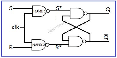
Here, we can observe that the SR flip-flop is constructed using an SR latch with NAND gates. Two additional NAND gates are connected to the inputs of the latch. Additionally, we can see the clock signal being applied to the inputs of the two NAND gates, and Q and Q̅ are the corresponding outputs.
Let’s consider that the output of the first NAND gate is denoted as S* and the output of the second NAND gate is denoted as R*.
Hence, we can express S* as S.clk bar, which can be simplified using DeMorgan’s law as S* = S̅ + clk bar.
Similarly, R* can be expressed as R.clk bar, and applying DeMorgan’s law yields R* = R̅+ clk bar.
And as we have studied above the truth table of SR latch using nand gate is as follows:

The SR flip-flop serves two primary functions:
- Set-Reset (SR) Operation: When the S input is set to 1, the output Q is also set to 1. Similarly, when the R input is set to 1, the output Q̅ is set to 1.
- Data Storage: The SR flip-flop is capable of storing a single bit of data. The current state of the flip-flop, represented by the outputs Q and Q̅, remains unchanged until a new input is received. This allows the flip-flop to retain its stored value, acting as a memory element for the stored bit.
The truth table of SR flip flop is as follow:

Now let us consider each case one by one:
1] clk = 0:
When clk input is 0 then according to the working of nand gate if any input is 0 then output is 1. Hence, irrespective of the S and R inputs S* and R* will be 1. Now if we consider the truth table of SR latch using Nand gate we can observe that when S* and R* both are equal to 1 then output is in memory state. Therefore, when clk is 0 Q and Q̅ will be in Memory state.
2] clk =1, S=0 and R=0:
Here, if we substitute the values of S, R and clk in the equations of S* and R* we get,
S* = S̅ + clkbar = 0̅ + 1̅ = 1 + 0 = 1 and
R* = R̅ + clkbar = 0̅ +1̅ = 1 + 0 = 1
and according to the truth table of SR latch, we can see that when S* = 1 and R* = 1 then Q and Q̅ are in memory state.
Therefore, when clk =1, S=0 and R=0 then Q and Q̅ are in memory state.
3] clk =1, S=0 and R =1:
Here, if we substitute the values of S, R and clk in the equations of S* and R* we get,
S* = S̅ + clkbar = 0̅ +1̅ = 1 + 0 = 1 and
R* = R̅ + clkbar = 1̅ +1̅ = 0 + 0 = 0
and according to the truth table of SR latch, we can see that when S* = 1 and R* = 0 then Q=0 and Q̅ is 1.
Therefore, when clk =1, S=0 and R=1 then Q=0 and Q̅ = 1
4] clk =1, S=1 and R =0:
Here, if we substitute the values of S, R and clk in the equations of S* and R* we get,
S* = S̅ + clkbar = 0̅ +1̅ = 0 + 0 = 0 and
R* = R̅ + clkbar = 1̅ +1̅ = 1 + 0 = 1
and according to the truth table of SR latch, we can see that when S* = 1 and R* = 0 then Q=1 and Q̅ is 0.
Therefore, when clk =1, S=1 and R=0 then Q=1 and Q̅ = 0.
5] clk =1, S=1 and R =1:
Here, if we substitute the values of S, R and clk in the equations of S* and R* we get,
S* = S̅ + clkbar = 1̅ +1̅ = 0 + 0 = 0 and
R* = R̅ + clkbar = 1̅ +1̅ = 0 + 0 = 0
and according to the truth table of SR latch, we can see that when S* = 0 and R* = 0 then Q and Q̅ are in invalid state.
Therefore, when clk =1, S=0 and R=0 then Q and Q̅ are in invalid state.
Now this truth table can also be written as follows where Qn+1 is the next state:
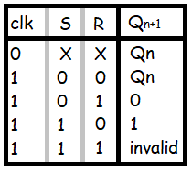
The characteristics table and excitation for SR flip flop is as follows:

2] D flip flop:
The below diagram shows circuit diagram for D flip flop:
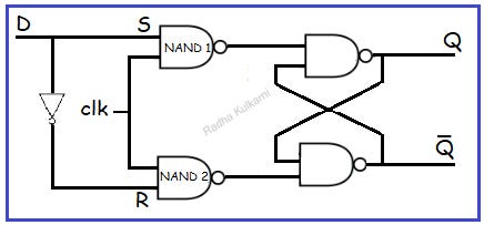
Here, we can observe that the D flip-flop is essentially an SR flip-flop with its input terminals connected together and an inverter circuit placed between them. It is also called as Delay or data flip flop. Additionally, we can see the clock signal being applied to the inputs of the two NAND gates, and Q and Q̅ are the corresponding outputs.
The D flip-flop serves two primary functions:
- Data Operation: When the D input is set to 1, the output Q is also set to 1. Similarly, when the D input is set to 1, then output Q is set to 1.
- Data Storage: The D flip-flop is capable of storing a single bit of data. The current state of the flip-flop, represented by the outputs Q and Q̅, remains unchanged until a new input is received. This allows the flip-flop to retain its stored value, acting as a memory element for the stored bit.
The truth table of D flip flop is as follow:

Now let us consider each case one by one:
1] clk = 0:
When clk input is 0 then according to the working of nand gate if any input is 0 then output is 1. Hence, irrespective of the D input output will be in memory state. Therefore, when clk is 0 Q and Q̅ will be in Memory state.
2] clk =1 and D =0:
As D input is set to 0 then S input will be 0 and R input will be 1 according to the inverting operation. And according to the truth table of SR flip flop, we can see that when S = 0 and R = 1 then Q and Q̅ are 0 and 1.
Therefore, when clk =1, D =0 then output (Qn+1) is 0.
3] clk =1, D =1:
As D input is set to 1 then S input will be 1 and R input will be 0 according to the inverting operation. And according to the truth table of SR flip flop, we can see that when S = 1 and R = 0 then Q and Q̅ are 1 and 0.
Therefore, when clk =1, D =1 then output (Qn+1) is 1.
The characteristics table and excitation for D flip flop is as follows :

3] JK flip flop:
The below diagram shows circuit diagram of JK flip flop.
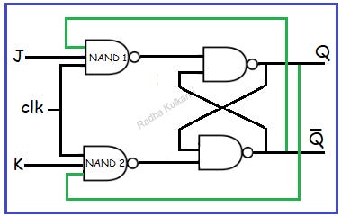
Here, you can observe that JK flip flop is essentially an SR flip flop with few modifications. In the JK flip flop, an additional feedback circuit is incorporated, where the output Q is connected to the input K and the output Q̅ is connected to the input J. In the case of an SR flip flop, we have observed that when both inputs are set to 1, an invalid output occurs. To prevent this invalid state, we utilize the JK flip flop. The operation of the JK flip flop is similar to that of an SR flip flop, except for the handling of the invalid state. Therefore, we will consider the invalid output state directly, as the remaining cases function in the same manner as an SR flip flop.
Now, let us see what the output will be when clk=1, J=1 and K=1. Let the previous state be where Q=1 and Q̅ =0. This Q̅ output will be given as feedback to J input and Q output to K input. We know that in case of NAND gate if any input is 0 then output will be 1. Hence, output of NAND gate 1 will be 1 and that of NAND gate 2 will be 0. As NAND gate 4 has one input as 0 its output will be 1 which will be given as feedback to NAND gate 3 and its output will be 0. Hence, now the outputs Q and Q̅ are 0 and 1 which as compliments of the previous outputs. Therefore, the output can be considered as memory bar when both inputs are equal to 1. In this way we can overcome the invalid state in SR flip flop by using JK flip flop.
The below diagram shows the truth tables for JK flip flop:

The characteristics table and excitation for JK flip flop are as follows:

What is Race around condition in JK flip flop??
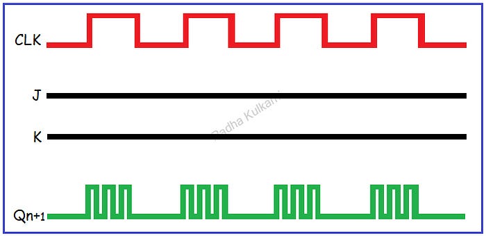
As explained above we can see how JK flip flop can be used to overcome the invalid state in SR flip flop when clk and both inputs are equal to 1. The output in this state will be memory bar in JK flip flop and not invalid output. But one thing we can notice here is that, if previous output is 0 and 1 then the output changes to 1 and 0 without any change in clock input i.e., the output is uncontrollable. The output gets toggled without changing the clk input. So, the feedback mechanism will follow again and again the output will keep on toggling irrespective of change in clk input. This can be referred as Race Around Condition.
This Race around condition can be summarized from the below waveform:
To avoid the Race Around Condition, the following solutions can be implemented:
- Using Edge Triggering
- Considering the race around time period or propagation delay (T’) and the total time period of a cycle (T), where the time period of the positive half cycle is T/2. If T’ is greater than T/2, the race around condition can be avoided. However, it is not practically possible to achieve this condition.
- Using Master and Slave Flip flop.
4] Master and Slave Flip flop:
Master and Slave flip flop can be used to avoid the race around condition occurring the JK flip flop. Here, we connect 2 flip flops Master and Slave in series with each other. The below diagram shows the circuit diagram of master and slave flip flop:
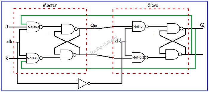
Let, the output of master flip flop be Qm and that of slave flip flop be Q. Output of master flip flop is connected to the input of slave flip flop. Both flip-flops share a common clock input, with an inverter placed between them. The feedback input for the Master flip-flop is obtained from the output of the Slave flip-flop, as shown in the diagram.
Now, let us see how master and slave can be used to avoid the race around condition:
When clk=1, J=1 and K=1, the clock input for slave flip flop (clk’) will be 0 due to the inverting operation between the clock inputs. Therefore, as per the working of JK flip flop, Master flip flop will be in Active state and Slave flip flop will be in memory state. Hence, no output change will occur in the output Q, thereby avoiding the occurrence of the race around condition.
Now, if we change the clock input (clk) to 0, then clk’ will become 1. In this scenario, the Master flip-flop will be in a memory state, and the Slave flip-flop will be in an active state according to the functioning of the JK flip-flop. Despite this, the output Q will remain unchanged since Qm is in a memory state, causing no alteration in the output and hence preventing the race around condition.
Please note that Master and slave flip flop is edge triggered flip flop.
To gain a clearer understanding of the operation, refer to the waveform diagram provided below.

As an edge-triggered flip-flop, the output changes occur at each transition from 0 to 1 or 1 to 0, not during level triggering. Consider the initial state where Qm is 0. It will change to 1 when the first clock edge is triggered and remain in that state until the next triggering event occurs. Similarly, the Q output will be triggered at each negative edge since the clock input for the Slave flip-flop is inverted. Consequently, the Q output will be triggered at each negative edge, ensuring that no race around condition occurs.
5] T flip flop:
The below diagram shows circuit diagram for T flip flop:

Here, we can observe that the T flip-flop is essentially an JK flip-flop with its input terminals connected together. It is also called as Toggle flip flop. Additionally, we can see the clock signal being applied to the inputs of the two NAND gates, and Q and Q̅ are the corresponding outputs.
And as we have studied above the truth table of JK flip flop using nand gate is as follows:

The T flip-flop serves two primary functions:
- Data Operation: When the T signal is set to a high state (1), it toggles the output signal. If the current output status is also high (1), it changes it to a low state (0). Conversely, if the current output status is low (0), it changes it to a high state (1).
- Data Storage: The T flip-flop is capable of storing a single bit of data. The current state of the flip-flop, represented by the outputs Q and Q̅, remains unchanged until a new input is received. This allows the flip-flop to retain its stored value, acting as a memory element for the stored bit.
The truth table of T flip flop is as follow:

Now let us consider each case one by one:
1] clk = 0:
When clk input is 0 then according to the working of nand gate if any input is 0 then output is 1. Hence, irrespective of the T input output will be in memory state. Therefore, when clk is 0 Q and Q̅ will be in Memory state.
2] clk =1 and T =0:
As T input is set to 0 then both J and K inputs will be 0. And according to the truth table of JK flip flop, we can see that when J = 0 and K = 0 then Q and Q̅ are in memory state.
Therefore, when clk =1, T =0 then output (Qn+1) is in memory state.
3] clk =1, T =1:
As T input is set to 1 then both J and K inputs will be 1. And according to the truth table of JK flip flop, we can see that when J = 0 and K = 0 then Q and Q̅ are in memory bar state.
Therefore, when clk =1, T =0 then output (Qn+1) is in memory bar state.
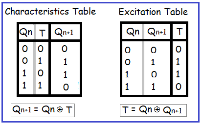
The characteristics table and excitation for T flip flop is as follows:
6] Preset and Clear Flip flop:
The basic operation of a preset and clear flip-flop is as follows: when a preset input is applied, the output Q becomes 1, and when a clear input is applied, the output Q becomes 0. These inputs provide predefined outputs regardless of the other inputs. The preset and clear inputs of the flip-flop are asynchronous, meaning they will have an immediate effect on the Q and Q̅ outputs regardless of the state of the clock and/or the inputs. These inputs are active low and are represented by a bubble in the flip-flop symbol.
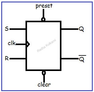
To understand the working of preset and clear inputs, let’s consider an SR flip-flop. The diagram below illustrates the use of preset and clear inputs with an SR flip-flop.
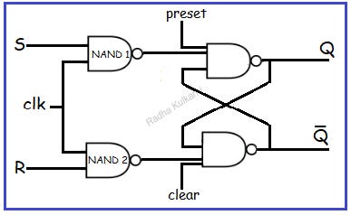
When the preset input is 0, according to the working of the NAND gate, the output Q will be 1. Similarly, when the clear input is 0, the output Q̅ will be 1, resulting in Q being 0.
In this way, regardless of the clock input or the S and R inputs, the preset and clear inputs will change the output.
The truth table for the preset and clear inputs is as follows:

In this way Flip flops can be used to store 1 bit of binary data.
No comments:
Post a Comment