- Flip-flops or latches are circuits that function as bistable multivibrators, capable of storing one bit of binary data. Once set to a particular state, they will remain in that state until directed by an input to change their state.
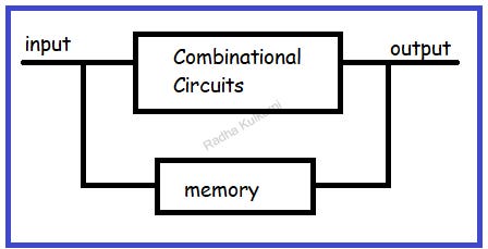
- They are classified as sequential circuits, which combine combinational circuits with memory elements. Combinational circuits produce output based solely on the current inputs, whereas sequential circuits produce output based on both current and past states.
- Below diagram shows block diagram of sequential circuits:
- Inorder to trigger the memory element in the sequential circuit we need clock. Operational speed and transition of state in sequential circuits can be defined by clock cycle.
- Let us take a look at a few concepts related to clock cycles before diving into the topic of flip flops:
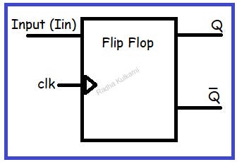
- Below diagram shows Block diagram of flip flop:
- Flip flops are of following types:
- D flip flop
- T flip flop
- SR flip flop
- JK flip flop
- Master and slave flip flop
- Difference between Latch and flip flop:
Below figure shows a basic clock cycle:

where,
Ton: time period when output is high
Toff: time period when output is low
T: Ton + Toff which is total time period for one cycle
Duty cycle (D): Ton/T
Frequency (F): 1/T
There are two types of clock triggering:
1) Edge Triggering:
- Positive Edge Trigger
- Negative Edge Trigger
2) Level Triggering
- Positive Level Trigger
- Negative Level Trigger
Hence, Flip flops can be defined as sequential circuits which can store one bit of data and are triggered using clock cycle.
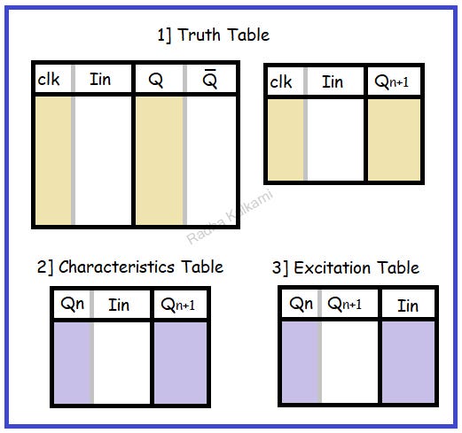
Below are few tables which will help us understand flip flops in detail:
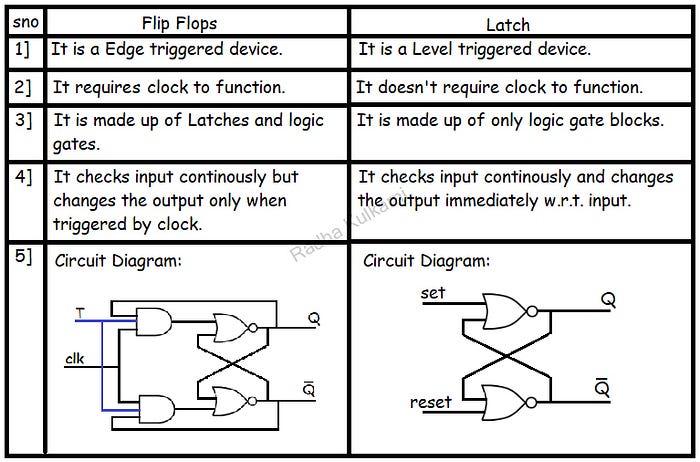
As a flip flop contains both latches and logic gates, let us first try to understand how a simple latch circuit works. The diagram below shows an SR (Set-Reset) latch.

Both latches and flip flops are used for storing memory, but latches do not have a clock input, and hence they deliver an output at all instances. In the SR latch using NOR gates, Q and Q̅ are the outputs, and R and S are the inputs. The output of one NOR gate is connected to the input of another NOR gate. Now, we will see the working of latches by considering a few cases.
We know that for a NOR gate, if any input is 1 then output is 0.
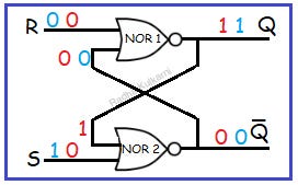
Case 1: S=1 and R=0
According to the working of the NOR gate, Q̅ will be 0, and this 0 will be given to NOR gate 1 as feedback, and hence Q will be 1. Therefore, when S=1 and R=0, then Q=1 and Q̅=0.
Case2: S=0 and R =0
Now, we have both inputs as 0, and the feedback input for NOR gate 1 is 0, and for NOR gate 2 is 1. Therefore, according to the functioning of the NOR gate, Q will be 1, and Q̅ will be 0.
For the above 2 cases, we can conclude that even if we change the inputs, the output remains constant, and in this way, we can store memory.
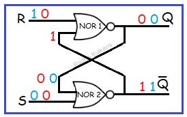
Case 3: S=0 and R=1
According to the working of the NOR gate, Q will be 0, and this 0 will be given to NOR gate 2 as feedback, and hence Q̅ will be 1. Therefore, when S=0 and R=1, then Q=0, and Q̅=1.
Case 4: S=0 and R =0
Now, we have both inputs as 0, and the feedback input for NOR gate 1 is 1, and for NOR gate 2 is 0. Therefore, according to the functioning of the NOR gate, Q will be 0, and Q̅ will be 1.
Similarly, from case 3 and case 4 we can conclude how latches can be used to store memory.
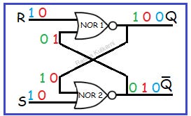
Case 5: Now we will consider a final case where both inputs S and R are 1. According to the working principle of NOR gate both Q and Q̅ will be 0 which is an invalid state as Q and Q̅ both are compliments of each other.
Now if we change both inputs to 0 then considering the feedback inputs for both NOR gate and we could possibly get two different output. First where Q is 0 and Q̅ is 1 and other where Q will be 1 and Q̅ 0.
Hence, when both inputs are 1 then latch will give an invalid output.
Now, considering above cases the truth table for SR latch using NOR gate will be as follow:

Similarly consider SR latch using NAND gate:
In the SR latch using NAND gates, Q and Q̅ are the outputs, and S and R are the inputs. The output of one NAND gate is connected to the input of another NAND gate. Now, we will see the working of latches by considering a few cases.
We know that for a NAND gate if any input is 0 then output will be 1.

Case 1: S=1 and R=0
According to the working of the NAND gate, Qbar will be 1, and this 1 will be given to NAND gate 1 as feedback, and hence Q will be 0. Therefore, when S=1 and R=0, then Q=0 and Q̅ =1.
Case2: S=1 and R =1
Now, we have both inputs as 0, and the feedback input for NAND gate 1 is 1, and for NAND gate 2 is 0. Therefore, according to the functioning of the NOR gate, Q will be 0, and Q̅ will be 1.
For the above 2 cases, we can conclude that even if we change the inputs, the output remains constant, and in this way, we can store memory.
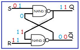
Case 3: S=0 and R=1
According to the working of the NAND gate, Q will be 1, and this 1 will be given to NAND gate 2 as feedback, and hence Q̅ will be 0. Therefore, when S=0 and R=1, then Q=1, and Q̅=0.
Case 4: S=1 and R =1
Now, we have both inputs as 0, and the feedback input for NAND gate 1 is 0, and for NAND gate 2 is 1. Therefore, according to the functioning of the NAND gate, Q will be 1, and Q̅ will be 0.
Similarly, from case 3 and case 4 we can conclude how latches can be used to store memory.

Case 5: Now we will consider a final case where both inputs S and R are 1. According to the working principle of NAND gate both Q and Q̅ will be 1 which is an invalid state as Q and Q̅ both are compliments of each other.
Now if we change the both inputs to 1 then considering the feedback inputs for both NAND gate and we could possibly get two different output. First where Q is 0 and Q̅ is 1 and other where Q will be 1 and Q̅ 0.
Hence, when both inputs are 1 then latch will give an invalid output.
Now, considering above cases the truth table for SR latch using NAND gate will be as follow:
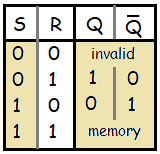
In my next blog, I will explain all Flip Flops in detail. So, stay tuned.
No comments:
Post a Comment