In this project, we will see how to implement all logic gates with verilog testbench code on Xilinx Vivado design tool. Below diagram shows all logic gates along with there truth tables, symbol and Boolean equation.
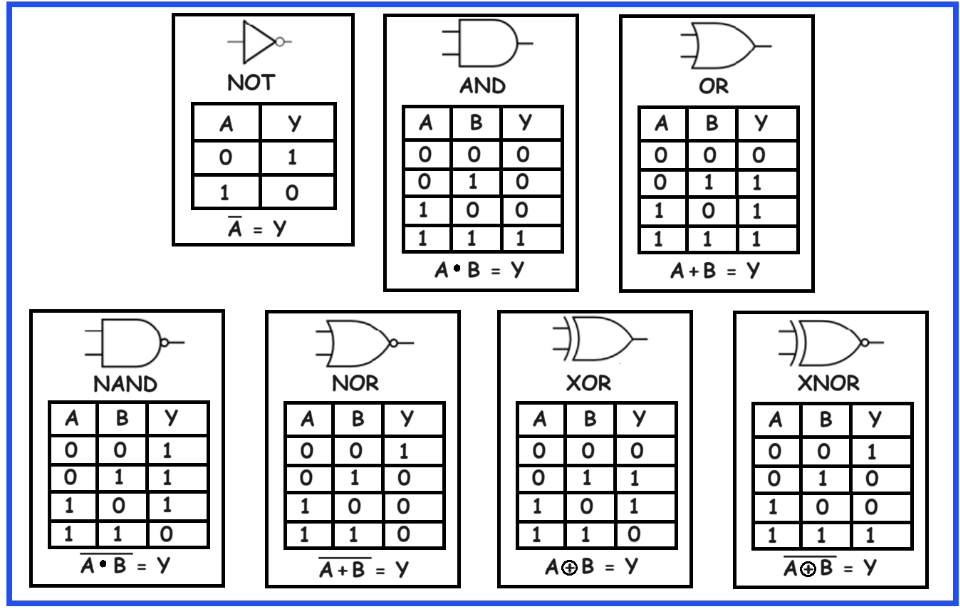
Now let us see how we will implement these gates using Xilinx Vivado design tool.
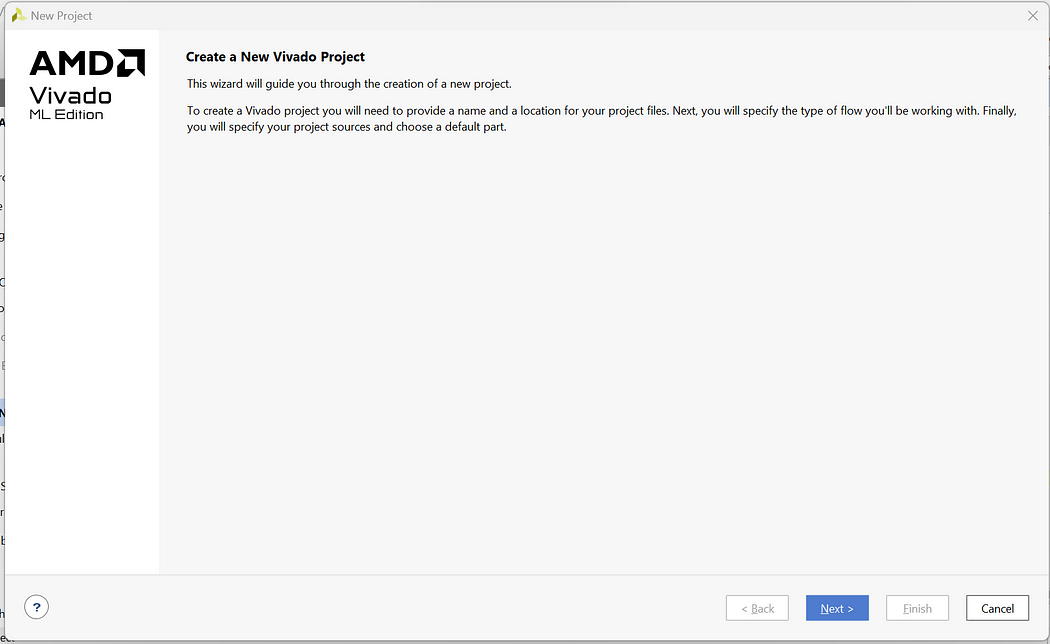
Step 1: Click on New Project -> Next
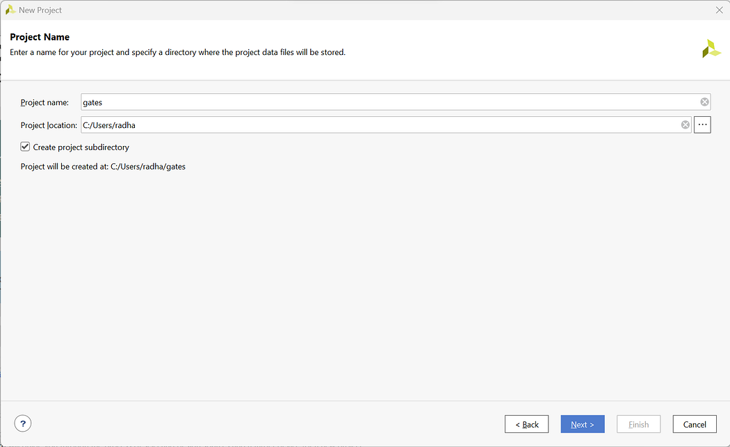
Step 2: Enter Project Name and Select appropriate Project Location -> Next
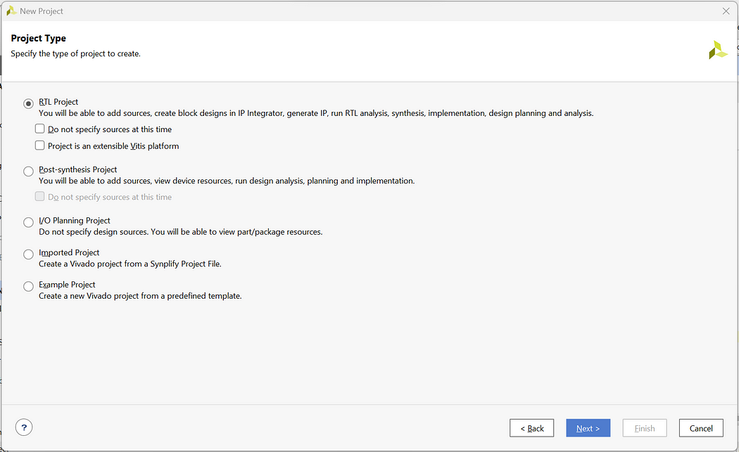
Step 3: Select RTL Project -> Next
Step 4: Click on Create File and create file with file name and_gate -> Next

Step 5: We will not add the Constraint file So click on Next
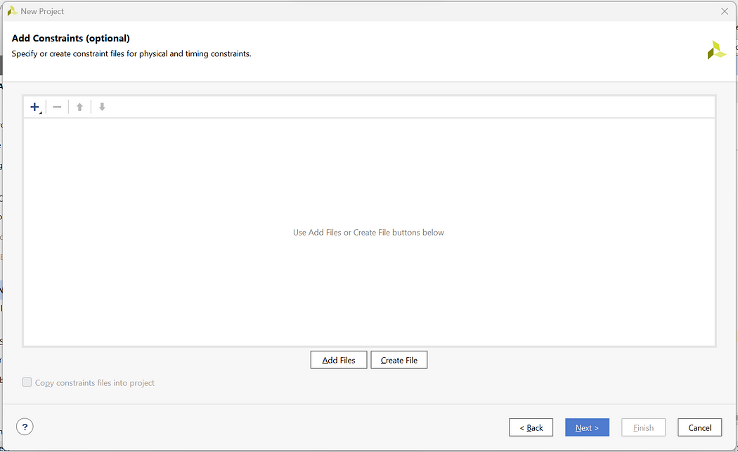
Step 6: For Default Part click on Next as we are not using any development Board
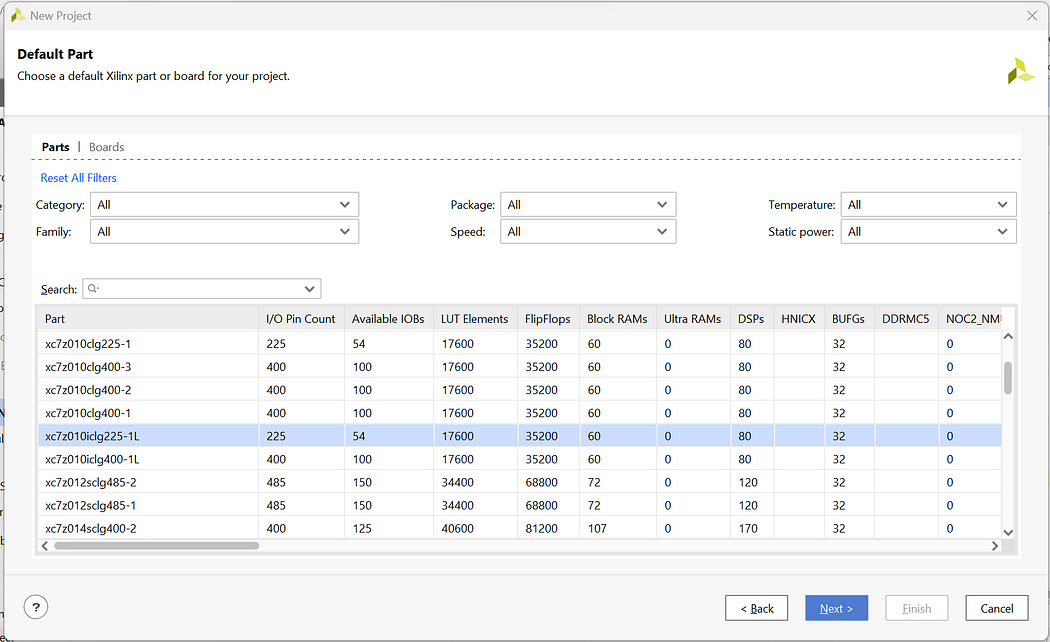
Step 7: Check the New Project Summary and click on Finish.

Step 8: Now you will be prompted with the Define module page but we will create the complete code from scratch so click on cancel and Yes
Step 9: Now on the Home Page click on Sources -> Design Sources -> Non-module Files

Step 10: Enter the below codes in the “and_gate.v” files.
and_gate.v
module and_gate(a,b,y);
input a;
input b;
output y;
and(y,a,b);
endmodule
Step 11: Now to write the testbench code for and gate right click on Design Sources -> Add Sources -> Add or create design sources -> Create File -> Add File name as tb_and_gate -> Finish -> Ok -> Yes
Step 12: Now open the testbench file and enter the below testbench code
module tb_and_gate;
reg a;
reg b;
wire y;
and_gate UUT (.a(a), .b(b), .y(y));
initial begin
$display(“Testing AND gate”);
a = 0; b=0;
#10;
$display(“Input_A = %b, Input_B = %b, Output = %b”, a,b,y);
a = 0; b=1;
#10;
$display(“Input_A = %b, Input_B = %b, Output = %b”, a,b,y);
a = 1; b=0;
#10;
$display(“Input_A = %b, Input_B = %b, Output = %b”, a,b,y);
a = 1; b=1;
#10;
$display(“Input_A = %b, Input_B = %b, Output = %b”, a,b,y);
$finish;
end
endmodule
Here, in testbench code we do not define values in entity hence we have kept it empty. Then in architecture we have copied the components of and_gate and defined signals for connecting the ports of and gate. Inside the process statement we write all 4 test cases from truth table and define the delay as 100ns.
Step 13: Now as we have written all the codes let’s launch the simulation. Enter launch_simulation in the Tcl Console and press Enter.
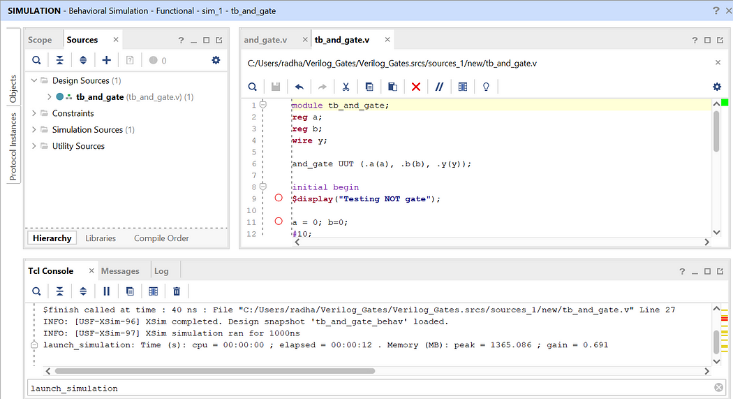
We have successfully implemented and gate with testbench code. Click on Zoom Fit to see the output waveform more clearly and verify the outputs.
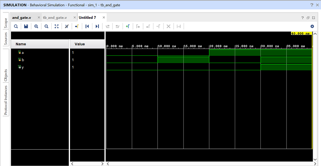
In this way, we can implement all logic gates using testbench codes.
No comments:
Post a Comment