In the field of integrated circuit (IC) fabrication, antenna effect is an important concept that needs to be understood and tackled effectively. This phenomenon occurs during plasma etching or dry etching, where metal or poly materials tend to accumulate charges that can subsequently flow through the gate oxide and damage it. As a result, this effect is known as Antenna Effect, as it resembles the behavior of an antenna in capturing charges.
Antenna Effect can also be referred to as Plasma Induced Gate Oxide Damage because the gate of the transistor usually gets damaged during plasma etching.
In IC fabrication, transistors are usually patterned during the Front End of Line (FEOL) process. This step involves patterning all individual components such as capacitors, resistors, and transistors on the semiconductor wafer. On the other hand, the Back End of Line (BEOL) step involves interconnecting these patterned components to the wafer using metallization.
Antenna Effect typically occurs during the BEOL process, which is an essential step in IC fabrication.
Dry or plasma etching is used to create a pattern on a substrate by selectively removing material from a thin film on the substrate. There are two types of etching: Wet etching and Dry/Plasma etching.
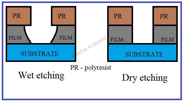
Wet etching involves the use of chemicals, while dry/plasma etching involves the use of stable gases. Antenna effect mainly occurs during dry etching, and not in wet etching, but dry etching is still preferred. Wet etching is isotropic in nature, which means that it will etch equally in both horizontal and vertical directions and result in an undercut. In contrast, dry/plasma etching is anisotropic in nature and will result in clean etching, as only the reactive area undergoes etching.
Plasma etching uses ionized gases (plasma) to etch materials on a wafer surface. The ions react with the material in specific regions to perform selective etching. Depending on the material, gases like CHF3 or SF6 can also be used in addition to CF4.
Results of both etching processes can be summarized in the below diagrams:

— What is Dry/Plasma etching??
Plasma is electrically neutral due to the presence of both positively charged ions and negatively charged electrons. Plasma etching, on the other hand, occurs in a chamber with two electrodes, one of which holds the wafer, and a high electric field is generated between them. Within this setup, a stable gas is introduced into the plasma, which reacts with the electrons and produces a byproduct that then reacts with the film and etches it. The most commonly used gas for etching silicon oxide is CF4 (tetrafluoromethane).
One unique aspect of plasma etching is that it only etches in a vertical direction as ions are bombarded from above, thereby making only a certain area reactive to undergo etching. This anisotropic characteristic of plasma etching is significant.
— Why do you have Antenna violation??

Antenna violations can occur if more conductor area is exposed to plasma, thereby accumulating more charge and discharging it through the gate oxide, leading to damage. The Antenna ratio, which is the ratio of the metal area connected to the gate to the total area of the gate, is an important consideration to avoid violations. Long metal lines and Vias can also introduce antenna violations, and it is crucial to fix them before chip tape-out.
Antenna Effect can result in gate oxide breakdown or threshold voltage shifts due to the accumulation and discharge of excessive charges through the gate. These failure mechanisms are crucial to understand.
— Methods to resolve antenna violations.
To resolve antenna violations, two common methods are typically used: Metal Jumpers and Adding Reversed Biased Diode near the gate.
- Metal Jumpers:
Metal Jumpers aim to avoid violations by breaking the metal near the gate and adding a jumper in higher metal layers. This process prevents charge accumulation and discharging through the gate during fabrication.
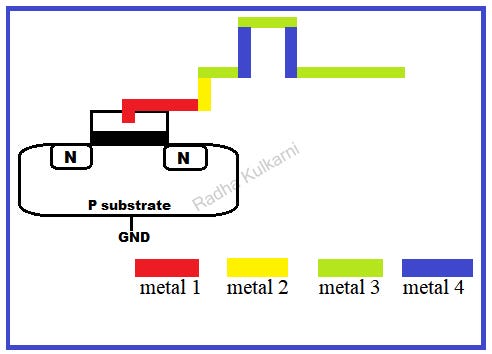
1)The figure below shows an NMOS with the gate connected to metals 1, 2, and 3. Metal 3 is higher than metals 1 and 2, indicating that antenna violations may occur on metal 3.

2) During fabrication, lower metals are fabricated first followed by higher metals. Metal 3 is long enough to accumulate sufficient charges to cause antenna violations. As diffusion is not yet formed for the rest of the part, the charges will discharge through the gate, leading to gate oxide destruction and antenna violation.
Higher metal layers are used because they are fabricated later in the process, reducing the likelihood of charge accumulation. Since the lower layers are already fabricated, charges from these layers may discharge through the gate if not addressed.
3)To solve this issue, metal jumpers are used in higher metal layers. The solution involves breaking the metal closest to the gate and adding a jumper in a higher metal layer. By breaking metal 3 and adding metal 4, then metal 3, and again metal 4, during fabrication, metal 4 is not yet fabricated, and the long wire of metal 3 will not be connected to the gate, preventing damage of the gate oxide and avoiding antenna violations. Once metal 3 is completely fabricated, the long metal will be safe from charge accumulation.

4)Now why only higher metal layers and not lower metal layers??
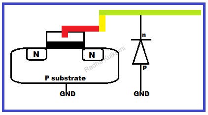
If lower metal layer, such as metal 2, is used, the path for metal 3 to discharge through the gate will still exist as metal 2 is already fabricated. This is illustrated in the diagram below.

- Diode Insertion:
Reversed-biased Diode Insertion involves adding a reversed-biased diode near the gate, which discharges charges onto the ground instead of the gate, thus avoiding antenna violations.

1)When the metal 3 collects a significant amount of charges, it will reach a specific potential. If this potential is equal to or greater than the breakdown potential of the reverse biased diode, then all the charges will be discharged through the diode into the ground. This prevents the charges from reaching the gate and causing antenna violations.
Reverse-biased diodes conduct only when the potential reaches a high breakdown voltage, safely discharging excess charge without affecting normal operation.
2)What will happen if we use forward biased diode instead of reverse biased diode to resolve antenna violations??

Reverse biased diode conduct at very high potential whereas forward biased diodes conduct at very lower potentials. Using a forward-biased diode can affect the normal operation of the circuit because the circuit typically works at lower potentials. Therefore, reversed-biased diodes are preferred for resolving antenna violations.
Alternative methods like dummy polysilicon routing or optimized metal routing can also minimize long metal paths and reduce the risk of antenna violations.
Antenna Effect is a significant challenge faced during IC fabrication, and implementing appropriate measures to prevent antenna violations is essential. Using Metal Jumpers or Adding Reversed Biased Diode near the gate are standard methods used to avoid antenna violations, and it is crucial to fix them before the chip tape-out to ensure high-quality IC fabrication.
No comments:
Post a Comment