- Transmission gate consists of a single nmos and pmos transistor, connected parallelly.
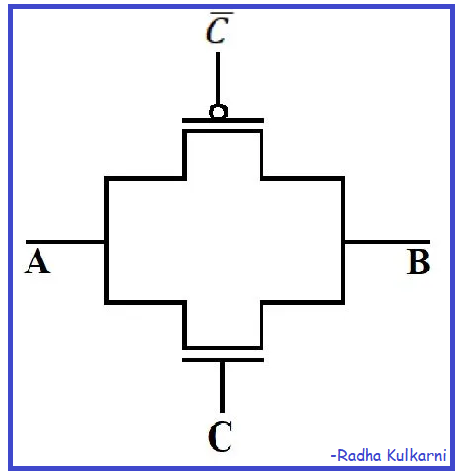
- Below figures shows the symbol of transmission gate CMOS.

- Here, A=input signal,
B=output signal,
C=control signal.
- Below figure shows the Basic Circuit Diagram of the CMOS transmission gate:

- It has one pmos and one nmos connected parallelly.
- Gate of pmos and nmos are complementary to each other which is the control signal.
— Working:
1] Here, we have 2 inputs A and C, and one output B where B=A.C .
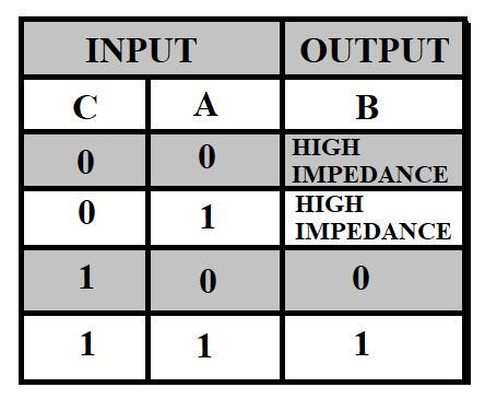
2] CASE-1: when C=0 and A=0 then according to the working of both transistors, both pmos and nmos will be in the OFF state and the circuit will act as an open circuit, and output B will be at a High Impedance state.
3] CASE-2: Similarly, when C=0 and A=1 both transistors will again be in the OFF state, and input A will have no effect on the output B will still be in the High Impedance state.
3] CASE-3: when C=1 and A=0 then according to the working of nmos and pmos, both transistors will be in ON state, and the circuit will act as a closed circuit. Here, even though both transistors are in the ON state still, input A=0 will pass through nmos as nmos is good to pass logic 0.
4] CASE-4: when C=1 and A=1 then according to the working of nmos and pmos, both transistors will be in ON state, and the circuit will act as a closed circuit. Here, even though both transistors are in the ON state still, input A=1 will pass through pmos as pmos is good to pass logic 1.
— Considering the below truth table for transmission gate CMOS, we can conclude that transmission gate CMOS can be used as a Tri-state buffer.

— Circuit design of 4:1 mux using transmission gate CMOS.
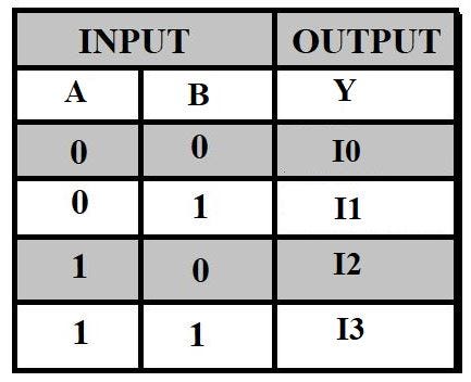
1] Consider 4:1 MUX with 4 inputs I0, I1, I2, I3, 2 select lines A and B, and output Y.

2] The below table shows the truth table for 4:1 MUX.

3] The Boolean equation Y will be
Y=Abar Bbar I0+Abar BI1+ ABbarI2+ABI3.
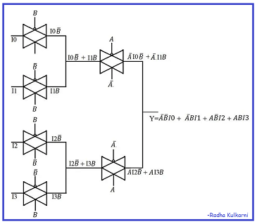
4] The below diagram shows the circuit design of the 4:1 mux using a transmission gate:

5] Here, we will have 4 transmission gates as 4 inputs and we will connect B select line input as the control input according to the output equation.
6] We know that the output of the transmission gate will be the product of the input and the control input. Hence, we will get the output of each transmission gate accordingly.
7] Now, we have another select line input A hence considering the Boolean equation we will connect 2 more transmission gates and connect the output of input transmissions gates to it to get the required output equation.
8] Hence, in this way we will design 4:1 MUX using transmission gate CMOS.
No comments:
Post a Comment